IC42S16100
Read Cycle (Full Page) Interruption Using
the Burst Stop Command
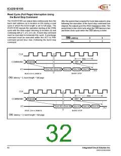
The IC42S16100 can output data continuously from the
burst start address (a) to location a+255 during a read
cycle in which the burst length is set to full page. The
IC42S16100 repeats the operation starting at the 256th
cycle with the data output returning to location (a) and
continuing with a+1, a+2, a+3, etc. A burst stop command
must be executed to terminate this cycle. A precharge
command must be executed within the ACT to PRE
command period (tRAS max.) following the burst stop
command.
After the period (tRBD) required for burst data output to stop
following the execution of the burst stop command has
elapsed, the outputs go to the HIGH impedance state. This
period (tRBD) is two clock cycle when the CAS latency is two
and three clock cycle when the CAS latency is three.
CAS Latency
3
2
tRBD
3
2
CLK
t
RBD
BST
COMMAND
I/O
READ A0
DOUT A0
D
OUT A0
DOUT A1
D
OUT A2
DOUT A3
HI-Z
BURST STOP
READ (CA=A, BANK 0)
CAS latency = 2, burst length = full page
CLK
t
RBD
BST
COMMAND
I/O
READ A0
DOUT A0
D
OUT A0
DOUT A2
DOUT A3
D
OUT A1
HI-Z
READ (CA=A, BANK 0)
BURST STOP
CAS latency = 3, burst length = full page
32
Integrated Circuit Solution Inc.
DR024-0D 06/25/2004

 ICSI [ INTEGRATED CIRCUIT SOLUTION INC ]