IC42S16100
Precharge
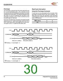
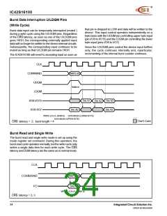
Read Cycle Interruption
Using the Precharge Command
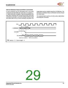
A read cycle can be interrupted by the execution of the
precharge command before that cycle completes. The
delay time (tRQL) from the execution of the precharge
command to the completion of the burst output is the clock
cycle of CAS latency.
The precharge command sets the bank selected by pin
A11 to the precharged state. This command can be
executed at a time tRAS following the execution of an active
command to the same bank. The selected bank goes to the
idle state at a time tRP following the execution of the
precharge command, and an active command can be
executed again for that bank.
If pin A10 is low when this command is executed, the bank
selected by pin A11 will be precharged, and if pin A10 is
HIGH, both banks will be precharged at the same time.
This input to pin A11 is ignored in the latter case.
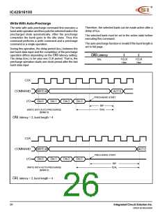
CAS Latency
3
3
2
2
tRQL
CLK
t
RQL
PRE 0
COMMAND
I/O
READ A0
DOUT A0
D
OUT A1
DOUT A2
HI-Z
READ (CA=A, BANK 0)
PRECHARGE (BANK 0)
CAS latency = 2, burst length = 4
CLK
t
RQL
PRE 0
COMMAND
I/O
READ A0
DOUT A0
D
OUT A1
D
OUT A2
HI-Z
READ (CA=A, BANK 0)
PRECHARGE (BANK 0)
CAS latency = 3, burst length = 4
30
Integrated Circuit Solution Inc.
DR024-0D 06/25/2004

 ICSI [ INTEGRATED CIRCUIT SOLUTION INC ]