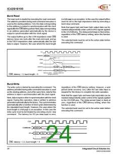
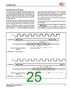
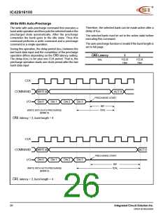
IC42S16100
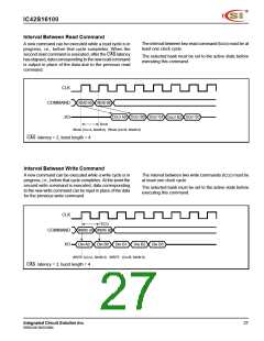
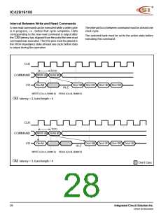
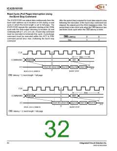
Interval Between Write and Read Commands
The interval (tCCD) between command must be at least one
clock cycle.
The selected bank must be set to the active state before
executing this command.
A new read command can be executed while a write cycle
is in progress, i.e., before that cycle completes. Data
corresponding to the new read command is output after
the CAS latency has elapsed from the point the new read
command was executed. The I/On pins must be placed in
the HIGH impedance state at least one cycle before data
is output during this operation.
CLK
t
CCD
COMMAND
I/O
WRITE A0 READ B0
DIN A0
DOUT B0
DOUT B1
D
OUT B2
DOUT B3
HI-Z
WRITE (CA=A, BANK 0) READ (CA=B, BANK 0)
CAS latency = 2, burst length = 4
CLK
t
CCD
COMMAND
I/O
WRITE A0 READ B0
DIN A0
DOUT B0
DOUT B1
D
OUT B2
DOUT B3
HI-Z
WRITE (CA=A, BANK 0) READ (CA=B, BANK 0)
CAS latency = 3, burst length = 4
Don’t Care
28
Integrated Circuit Solution Inc.
DR024-0D 06/25/2004

 ICSI [ INTEGRATED CIRCUIT SOLUTION INC ]