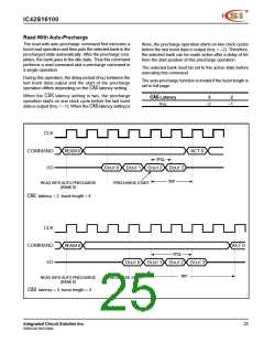
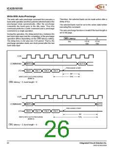
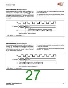
IC42S16100
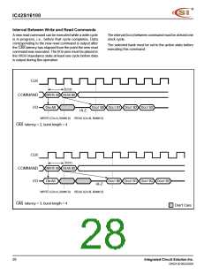
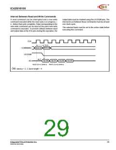
Interval Between Read and Write Commands
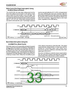
A read command can be interrupted and a new write
command executed while the read cycle is in progress, i.
e., before that cycle completes. Data corresponding to the
new write command can be input at the point new write
command is executed. To prevent collision between input
and output data at the I/On pins during this operation, the
output data must be masked using the U/LDQM pins. The
interval (tCCD) between these commands must be at least
one clock cycle.
The selected bank must be set to the active state before
executing this command.
CLK
tCCD
WRITE B0
COMMAND
U/LDQM
I/O
READ A0
HI-Z
DIN B0
DIN B1
DIN B2
DIN B3
READ (CA=A, BANK 0) WRITE (CA=B, BANK 0)
CAS latency = 2, 3, burst length = 4
Integrated Circuit Solution Inc.
29
DR024-0D 06/25/2004

 ICSI [ INTEGRATED CIRCUIT SOLUTION INC ]