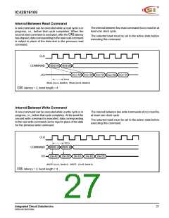
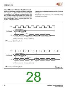
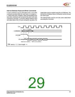
IC42S16100
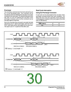
Write Cycle Interruption Using the
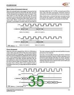
Precharge Command
A write cycle can be interrupted by the execution of the
precharge command before that cycle completes. The
delay time (tWDL) from the precharge command to the point
where burst input is invalid, i.e., the point where input data
is no longer written to device internal memory is zero clock
cycles regardless of the CAS.
Inversely, to write all the burst data to the device, the
precharge command must be executed after the write data
recovery period (tDPL) has elapsed. Therefore, the
precharge command must be executed on one clock cycle
that follows the input of the last burst data item.
To inhibit invalid write, the DQM signal must be asserted
CAS Latency
3
0
1
2
0
1
HIGH with the precharge command.
tWDL
This precharge command and burst write command must
be of the same bank, otherwise it is not precharge interrupt
but only another bank precharge of dual bank operation.
tDPL
CLK
tWDL=0
PRE 0
COMMAND
WRITE A0
DQM
I/O
DIN A0
DIN A1 DIN A2
DIN A3
MASKED BY DQM
PRECHARGE (BANK 0)
WRITE (CA=A, BANK 0)
CAS latency = 2, 3, burst length = 4
CLK
tDPL
PRE 0
COMMAND
I/O
WRITE A0
DIN A0
DIN A1
DIN A2
DIN A3
WRITE (CA=A, BANK 0)
PRECHARGE (BANK 0)
CAS latency = 2, 3, burst length = 4
Integrated Circuit Solution Inc.
31
DR024-0D 06/25/2004

 ICSI [ INTEGRATED CIRCUIT SOLUTION INC ]