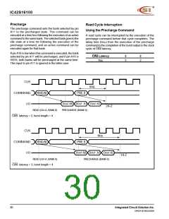
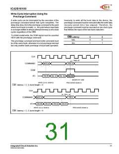
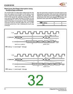
IC42S16100
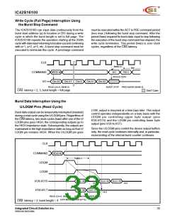
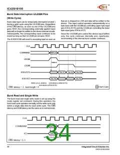
Burst Data Interruption U/LDQM Pins
(Write Cycle)
Burst data input can be temporarily interrupted (muted )
during a write cycle using the U/LDQM pins. Regardless
of the CAS latency, as soon as one of the U/LDQM pins
goes HIGH, the corresponding externally applied input
data will no longer be written to the device internal circuits.
Subsequently, the corresponding input continues to be
muted as long as that U/LDQM pin remains HIGH.
that pin is dropped to LOW and data will be written to the
device. This input control operates independently on a
byte basis with the UDQM pin controlling upper byte input
(pin I/O8 to I/O15) and the LDQM pin controlling the lower
byte input (pins I/O0 to I/O7).
Since the U/LDQM pins control the device input buffers
only, the cycle continues internally and, inparticular,
incrementing of the internal burst counter continues.
The IC42S16100 will revert to accepting input as soon as
CLK
COMMAND
UDQM
WRITE A0
tDMD=0
LDQM
I/O8-I/O15
I/O0-I/O7
DIN A1
DIN A3
DIN A3
DIN A2
DIN A0
WRITE (CA=A, BANK 0)
DATA MASK (LOWER BYTE)
CAS latency = 2, burst length = 4DATA MASK (UPPER BYTE)
Don’t Care
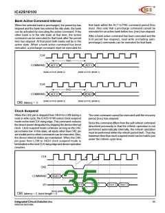
Burst Read and Single Write
The burst read and single write mode is set up using the
mode register set command. During this operation, the
burst read cycle operates normally, but the write cycle only
writes a single data item for each write cycle. The CAS
latency and DQM latency are the same as in normal mode.
CLK
COMMAND
WRITE A0
DIN A0
I/O
WRITE (CA=A, BANK 0)
CAS latency = 2, 3
34
Integrated Circuit Solution Inc.
DR024-0D 06/25/2004

 ICSI [ INTEGRATED CIRCUIT SOLUTION INC ]