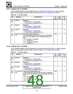
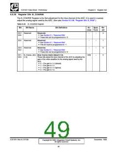
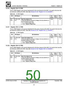
ICS1531 Data Sheet - Preliminary
Chapter 6 Register Set
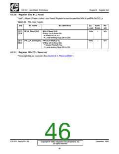
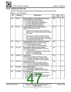
6.5.32 Register 30h: ADC CTRL
The ADC CTRL (Analog-to-Digital Converter Control) Register is used to control the ADC.
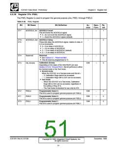
Table 6-31. ADC CTRL Register
Bit
Bit Name
Bit Definition
Ac- Spec.
cess Func.
Re-
set
30:7
ADC_OE
Analog-to-Digital Converter (Digital) Outputs Enable.
R/W
–
0
T•his0b=itTehneabAlDesCthdeigAitaDlCoudtipguittaslaoruetpduistsa.bled.
(The ICS1531 output pads are high-impedance.)
• 1 = The ADC digital outputs are enabled.
(The polarity is controlled by Reg 30:5.)
30:6
ADC_Sel
Analog-to-Digital Converter (Capture) Select.
R/W
–
0
T•his0b=it selects a mode for the ADC.
– The clock rate is 2 pixels per clock (half-rate clock).
– Both the ‘A’ and ‘B’ channels each provide 24-bit pixels
(48 bits total).
• 1 =
– The clock rate is 1 pixel per clock (full-rate clock).
– The ‘A’ channel provides 24-bit pixels (24 bits total).
– The ‘B’ channel is driven either high or low, depending
on the value of Reg 30:5 (ADC_INV).
30:5
30:4
ADC_Inv
Analog-to-Digital Converter (Output) Invert (Disable).
R/W
R/W
–
–
1
0
T•his0b=itTdhiseaAblDeCs tohuetpinuvtesrasrioeninovfetrhteedA.DC outputs.
• 1 = The ADC outputs are not inverted (default).
Force_ADC
Force Analog-to-Digital Converter (Outputs).
T•his0b=itNfoorrcmeasltoop‘oefrfa’taiollnoutput buffers for the ADC pin.
• 1 = Force all ADC output buffers low or high as follows:
– Reg 30:5 = 0 to force buffers low
– Reg 30:5 = 1 to force buffers high
30:3
30:2
CLAMP_Pol
CLAMP_Sel
Clamp Polarity.
R/W
R/W
–
–
0
0
T•his0b=itTsheelepcotslatrhiteypoofltahreitysiogfntahletosiagncalal mtopaisclpaomspit.ive.
• 1 = The polarity of the signal to a clamp is negative.
Clamp (Source) Select.
T•his0b=itTsheelescotsurthcee osof uthrecesiogfntahleissiignntearlntaollay cgleanmepra. ted.
• 1 = The source of the signal is from the CLAMP pin.
V•ide0o=AVmidpeloifaiemrpDliifsiearbilsee. nabled (default).
30:1
30:0
VA_Disable
FA_Disable
–
–
–
0
0
• 1 = Video amplifier is disabled to conserve power.
F•ine0 A=dTjhuestDDAiCsasbalree. enabled and they drive the VRTR,
R/W
VRTG, and VRTB pins internally.
• 1 = The DACs are disabled and the VRTR, VRTG, and
VRTB pins must be driven externally with ADC top
reference voltage.
ICS1531 Rev N 12/1/99
December, 1999
Copyright © 1999, Integrated Circuit Systems, Inc.
All rights reserved.
47

 ICSI [ INTEGRATED CIRCUIT SOLUTION INC ]