ICS1531 Data Sheet - Preliminary
Chapter 6 Register Set
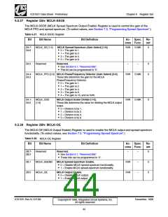
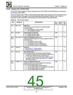
6.5.29 Register 2Ch: OUTPUT MUX
The OUTPUT MUX Register is used to select the source for the REF pin and STATUS pin (an active-low
pin formerly called ‘LOCK’).
Table 6-29 refers to ADC_FUNC, an internally generated signal that is delayed so it is in the same domain
as the internal ADC_CLK signal. Functionally, depending on the setting of Reg 06:3, ADC_FUNC is
equivalent to either ADCSYNC (which provides recovered HSYNC) or the input HSYNC.
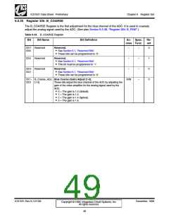
Table 6-29. OUTPUT MUX Register
Bit
Bit Name
Bit Definition
Ac- Spec. Re-
cess Func.
set
2C:7
High_Drive
High Drive.
–
–
0
This bit selects a drive strength for all analog-to-digital
converter outputs.
• 0 = Drive strength is normal strength.
• 1 = Drive strength is doubled.
O•ut0pu=tDEisnaabblleeOfoSrCOOSUCTOoUuTtp. ut.
• 1 = Enable OSCOUT output.
OSCOUT (Multiplexer) Select [1-0].
These bits select the output from a 4-way multiplexer (MUX) to
the OSCOUT pin.
2C:6
OE_OSC
R/W
R/W
–
–
1
0
2C:5-
2C:4
OSC_Sel [1-0]
• 0 = The OSCOUT source is OSC.
• 1 = The OSCOUT source is OSC/2.
• 2 = The OSCOUT source is OSCDIVIDER.
• 3 = The OSCOUT source is a reserved value.
R•esSeerveeSde.ction 6.1, “Reserved Bits”.
• This bit must be programmed to ‘0’.
2C:3
2C:2
Reserved
REF_Sel
–
–
–
0
0
REF (Status) Select.
R/W
T•his0b=itTsheeleRcEtsFthoeutRpuEtFsopuinrcreefiesrfernocmetohuetipnuptuatstofothlleowpsix:el PLL
PDINPUT (the Phase/Frequency Detector Input).
• 1 = The REF output source is from ADC_FUNC. (For more
information on ADC_FUNC, see Section 6.5.7, “Register
06h: Output Enables”.)
2C:1-
2C:0
LCKSEL [1-0]
(PLL) Lock (Status) Select [1-0].
These bits select the lock status output for the active-low
R/W
–
1
S•TA0T=USThpeinlo(fcokrmsteartluyscoaulltepdut‘LisOfCoKr ’t.h)e pixel PLL.
• 1 = The lock status output is for the Dynamic Phase Adjust.
• 2 = The lock status output is for PNLCLK.
• 3 = The lock status output is for MCLK.
ICS1531 Rev N 12/1/99
December, 1999
Copyright © 1999, Integrated Circuit Systems, Inc.
All rights reserved.
45

 ICSI [ INTEGRATED CIRCUIT SOLUTION INC ]