ICS1531 Data Sheet - Preliminary
Chapter 6 Register Set
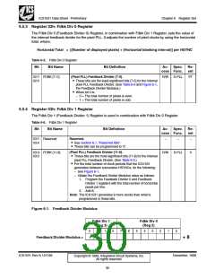
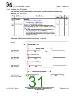
6.5.5 Register 04h: DPA Offset
The DPA Offset (Dynamic Phase Adjust Offset) Register is used to select the clock edge offset.
Table 6-7. DPA Offset Register
Bit
Bit Name
Bit Definition
Ac- Spec. Re-
cess Func.
set
R•esSeerveeSde.ction 6.1, “Reserved Bits”.
• These bits can be programmed to ‘0’.
04:7- Reserved
04:6
–
–
0
04:5- DPA_OS [5-0]
04:0
Dynamic Phase Adjust Offset [5-0].
R/W
–
0
As Figure 6-2 shows, these bits control the amount of offset
between the rising edge of the recovered HSYNC and the rising
edge of CLK.
• The offset is in discrete steps from 0 clock periods up to 1
clock period, minus one unit of a DPA delay.
• The unit of the DPA delay depends on both the pixel clock
output frequency and the number of delay element units (as
selected by Reg 05:1-0).
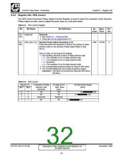
Figure 6-2. DPA Offset (As Determined by Regs 04 and 05)
HSYNC
Fixed delay ≈ 2.5 ns
One clock period
CLK Offset when
DPA_OS [5-0] = 0
t
t
Low
High
1 unit of DPA delay
CLK Offset when
DPA_OS [5-0] = 1
t
High
2 units of DPA delay
CLK Offset when
DPA_OS [5-0] = 2
t
High
.
.
.
.
.
.
Maximum units of DPA delay
One unit of
CLK Offset when
t
High
DPA Delay
DPA_OS [5-0] = Max
ICS1531 Rev N 12/1/99
December, 1999
Copyright © 1999, Integrated Circuit Systems, Inc.
All rights reserved.
31

 ICSI [ INTEGRATED CIRCUIT SOLUTION INC ]