ICS1531 Data Sheet - Preliminary
Chapter 6 Register Set
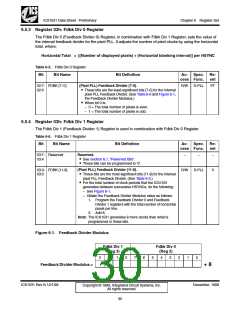
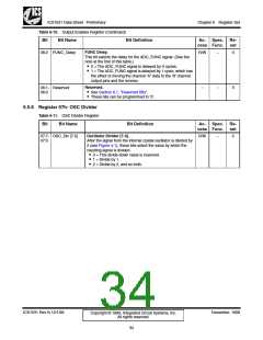
6.5.3 Register 02h: Fdbk Div 0 Register
The Fdbk Div 0 (Feedback Divider 0) Register, in combination with Fdbk Div 1 Register, sets the value of
the internal feedback divider for the pixel PLL. It adjusts the number of pixel clocks by using the horizontal
total, where:
Horizontal Total = [(Number of displayed pixels) + (Horizontal blanking interval)] per HSYNC
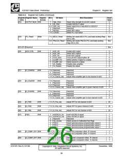
Table 6-5. Fdbk Div 0 Register
Bit
Bit Name
Bit Definition
Ac- Spec. Re-
cess Func.
set
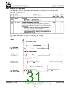
02:7- FDBK [7–0]
02:0
(Pixel PLL) Feedback Divider [7-0].
• These bits are the least-significant bits [7-0] for the internal
pixel PLL Feedback Divider. (See Table 6-6 and Figure 6-1,
the Feedback Divider Modulus.)
R/W D-PLL
FF
• When bit 0 is:
– 0 = The total number of pixels is even.
– 1 = The total number of pixels is odd.
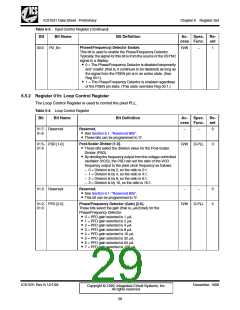
6.5.4 Register 03h: Fdbk Div 1 Register
The Fdbk Div 1 (Feedback Divider 1) Register is used in combination with Fdbk Div 0 Register.
Table 6-6. Fdbk Div 1 Register
Bit
Bit Name
Bit Definition
Ac- Spec. Re-
cess Func.
set
R•esSeerveeSde.ction 6.1, “Reserved Bits”.
• These bits can be programmed to ‘0’.
03:7- Reserved
03:4
–
–
–
03:3- FDBK [11-8]
03:0
(Pixel PLL) Feedback Divider [11-8].
R/W
D-PLL
0
• These bits are the most-significant bits [11-8] for the internal
pixel PLL Feedback Divider. (See Table 6-5.)
• For the total number of clock periods that the ICS1531
generates between successive HSYNCs, do the following:
– See Figure 6-1.
– Obtain the Feedback Divider Modulus value as follows:
1. Program the Feedback Divider 0 and Feedback
Divider 1 registers with the total number of horizontal
pixels per line.
2. Add 8.
Note: The ICS1531 generates 8 more clocks than what is
programmed in these bits.
Figure 6-1. Feedback Divider Modulus
Fdbk Div 1
(Reg 3)
Fdbk Div 0
(Reg 2)
3
2
1
0
7
6
5
4
3
2
1
0
Feedback Divider Modulus =
+ 8
ICS1531 Rev N 12/1/99
December, 1999
Copyright © 1999, Integrated Circuit Systems, Inc.
All rights reserved.
30

 ICSI [ INTEGRATED CIRCUIT SOLUTION INC ]