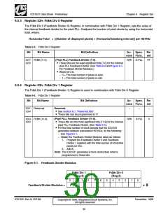
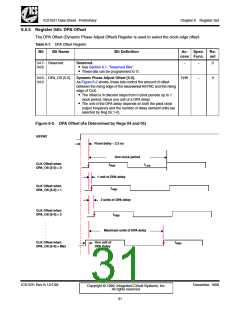
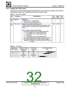
ICS1531 Data Sheet - Preliminary
Chapter 6 Register Set
Table 6-10. Output Enables Register (Continued)
Bit
Bit Name
Bit Definition
Ac- Spec. Re-
cess Func.
set
06:2 FUNC_Delay
FUNC Delay.
R/W
–
0
This bit selects the delay for the ADC_FUNC signal. (See the
n•ote0a=t TthheefAirsDtCo_f FthUisNtCabsleig.n) al is delayed by 0 cycles.
• 1 = The ADC_FUNC signal is delayed by 1 cycle, which has
the effect of moving the channel ‘A” data to the ‘B’ channel
output pins and the reverse.
R•esSeerveeSde.ction 6.1, “Reserved Bits”.
• These bits can be programmed to ‘0’.
06:1- Reserved
06:0
–
–
0
6.5.8 Register 07h: OSC Divider
Table 6-11. OSC Divider Register
Bit
Bit Name
Bit Definition
Ac- Spec. Re-
cess Func.
set
07:7- OSC_Div [7-0]
07:0
Oscillator Divider [7-0].
R/W
–
0
After the signal from the internal crystal oscillator is divided by
2 (see Figure 4-1), these bits select the value by which the
resulting signal is divided.
• 0 = This divide-down value is reserved.
• 1 = Divide by 1.
• 2 = Divide by 2, and so forth.
ICS1531 Rev N 12/1/99
December, 1999
Copyright © 1999, Integrated Circuit Systems, Inc.
All rights reserved.
34

 ICSI [ INTEGRATED CIRCUIT SOLUTION INC ]