IBM3009K2672
IBM SONET/SDH Framer
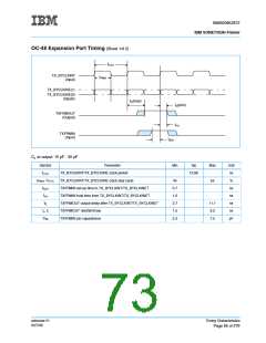
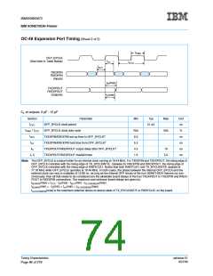
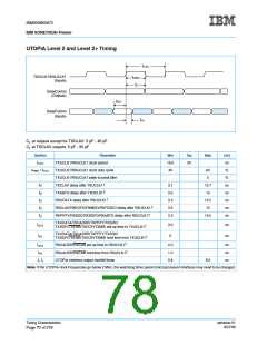
OC-48 Expansion Port Timing (Sheet 2 of 2)
tPWH
OFP_BYCLK
(See Note in Table Below)
tH1
tCYC
tSU1
TXEXPIN
RXEXPIN
(Inputs)
tD(max)
tD(min)
TXEXPOUT
RXEXPOUT
(Outputs)
C at outputs: 3 pF - 12 pF
L
Symbol
tCYC
Parameter
Min
Typ
Max
N/A
Unit
ns
%
OFP_BYCLK clock period
51.44
tPWH / tCYC
OFP_BYCLK clock duty cycle
N/A
6.0
5.5
4.5
1.3
tSU1
tH1
tD
TXEXPIN/RXEXPIN set-up time to OFP_BYCLK↑
TXEXPIN/RXEXPIN hold time from OFP_BYCLK↑
ns
ns
ns
ns
TXEXPOUT/RXEXPOUT output delay after OFP_BYCLK↑
19
tr, tf
TXEXPOUT/RXEXPOUT rise/fall times
5.0
Note: The OFP_BYCLK is a place holder for an internal clock running at 19.44 MHz. For TXEXPIN and TXEXPOUT, the rising edge of
OFP_BYCLK coincides with the rising edge of TX_BYCLKINT/E. Likewise for RXEXPIN and RXEXPOUT, the rising edge of
OFP_BYCLK coincides with the rising edge of RXBYCLK1. Notice that both RXBYCLK1 and TX_BYCLKINT/E operate at
77.76 MHz while OFP_BYCLK operates at 19.44 MHz. In both cases, the phase between the internal OFP_BYCLK and the
external clock can vary in multiples of 12.86 ns. As long as the internal OFP clocks of the four SONET/SDH framers run syn-
chronously, then all that needs to be considered are the allowable board delays of the four TXEXPOUT to TXEXPIN and RXEX-
POUT to RXEXPIN connections. The maximum and minimum board delays are given by:
tBOARD(max) = tCYC - tD(max) - tSU1(min) - tCLOCKSKEW(max)
tBOARD(min) = - tD(min) + tH1(min) + tCLOCKSKEW(max)
tCLOCKSKEW(max) is the maximum external device-to-device skew of TX_BYCLKINT/E or RXBYCLK1 on the board.
Timing Characteristics
Page 66 of 279
ssframer.01
8/27/99

 IBM [ IBM ]