IBM3009K2672
IBM SONET/SDH Framer
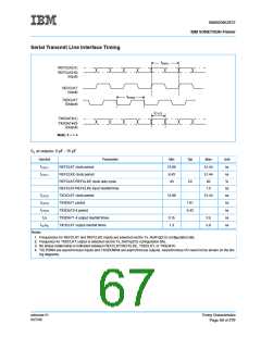
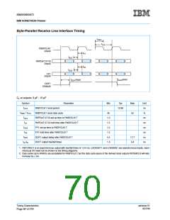
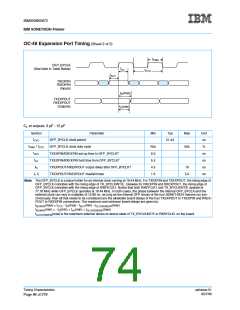
Byte-Parallel Receive Line Interface Timing
tPWH
tCYC
RXBYCLK1
(Input)
tH1
tSU1
RXPDAT1(7:0)
(Input)
tH2
tSU2
FP1
(Input)
tDOF(min)
tDOF(max)
OOF1
(Output)
C at outputs: 3 pF - 15 pF
L
Symbol
tCYC
Parameter
Min
Typ
Max
55
Unit
ns
%
RXBYCLK1 clock period
12.86
tPWH / tCYC
tSU1
RXBYCLK1 clock duty cycle
45
1.0
1.5
1.0
1.5
4.5
1.3
RXPDAT1(7:0) set-up time to RXBYCLK1↑
RXPDAT1(7:0) hold time after RXBYCLK1↑
FP1 set-up time to RXBYCLK1↑
ns
ns
ns
ns
ns
ns
tH1
tSU2
tH2
FP1 hold time after RXBYCLK1↑
tDOF
OOF1 output delay after RXBYCLK1↑
OOF1 output rise/fall times
17.7
5.8
trC,tfC
1. RSTCREC1 is an asynchronous output with rise/fall times of 1.2-5 ns. LOCKDET1 and LOSSSIG1 are asynchronous inputs. Asyn-
chronous I/O need not be shown on the timing diagrams.
2. Duty cycles up to 40/60% are acceptable for RXBYCLK1; but the duty cycle specs of the derived clock outputs RXTB#CLK will also
increase by 5%.
Timing Characteristics
Page 62 of 279
ssframer.01
8/27/99

 IBM [ IBM ]