IBM3009K2672
IBM SONET/SDH Framer
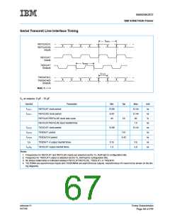
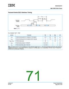
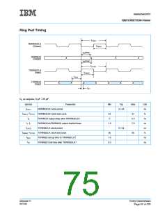
Transmit Serial DCC Interface Timing
tCYC
tPWL
tPWH
T1DCLK#
(Output)
tH1
tSU1
T1DATA#
(Input)
Note: # = 1-4
C at outputs: 3 pF - 15 pF
L
Symbol
Parameter
Min
Typ
5.21
1.73
Max
5.25
1.75
55
Unit
µs
µs
%
tCYC
tCYC
tPWH / tCYC
tSU1
T1DCLK# clock period for 192 kbit/s D1-D3 channel
T1DCLK# clock period for 576 kbit/s D4-D12 channel
T1DCLK# duty cycle
5.19
1.7
45
T1DATA# set-up time to T1DCLK#↑
T1DATA# hold time after T1DCLK#↑
2 x 51.44
1 x 51.44
ns
ns
tH1
Note: The timing shown is for the EdgeMode bit of the OT#Conf7 register set to ‘1’. The timing parameters remain the same when the
EdgeMode bit is set to ’0’, except that T1DATA# is sampled on the falling edge of the corresponding T1DCLK#. Each TX Serial DCC
interface can be individually configured.
ssframer.01
8/27/99
Timing Characteristics
Page 63 of 279

 IBM [ IBM ]