IBM3009K2672
IBM SONET/SDH Framer
Timing Characteristics
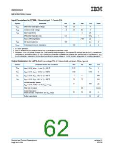
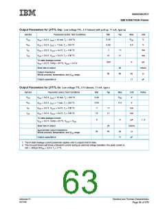
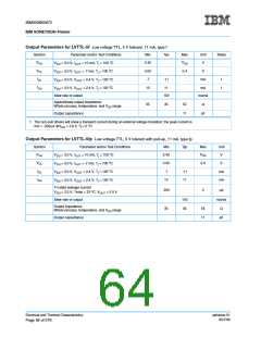
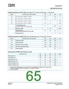
This section presents the detailed timing characteristics for the SONET/SDH framer. The load capacitances
for the output times are indicated in each figure as applicable. Unless otherwise indicated, timing parameters
are measured at specific signal voltage levels:
TTL Inputs
-
-
-
-
-
.8 / 2.0 V
.8 / 2.0 V
V-crosspoint to V-crosspoint
V-crosspoint to V-crosspoint
V-crosspoint to V-crosspoint
TTL Outputs
LPECL Inputs
PPECL Inputs
PPECL Outputs
The specifications given in this section cover two sets of environmental conditions:
ο
ο
Set 1: T = 0 C to 100 C, V = 3.3 V 0.3 V
j
DD
ο
ο
Set 2: T = -40 C to 125 C, V = 3.3 V 5%
j
DD
Note: Temperature and power supply conditions of the two sets above must not be mixed. Measurements
assume input rise and fall times of 2 ns (except REFCLKT/REFCLKE/RXSDAT1(0:1)). Lower and upper lim-
its for the pin capacitance C at the outputs are specified for each interface. All drivers are 50 Ω source-termi-
L
nated. Impedance-matched interconnections are assumed.
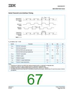
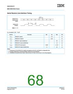
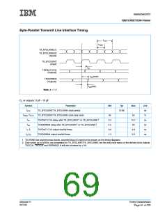
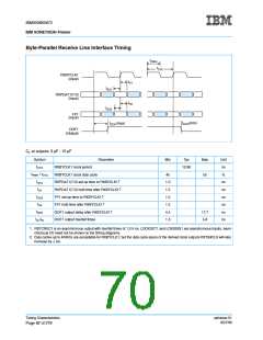
In all timing diagrams the # symbol is used as an index and takes on the values 1-4. For instance, T1DCLK#
is used to compactly represent T1DCLK1, T1DCLK2, T1DCLK3, and T1DCLK4.
Timing Characteristics
Page 58 of 279
ssframer.01
8/27/99

 IBM [ IBM ]