APCPCWM_4828539:WP_0000001WP_0000001
1
H27(U_S)4G8_6F2D
4 Gbit (512M x 8 bit) NAND Flash
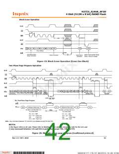
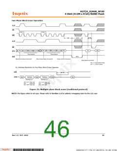
Two-Plane Block Erase Operation
CLE
CE
tWC
tWC
WE
tWHR
tWB
tBERS
ALE
RE
62ꢇ Roꢆ Add1 Roꢆ Add±
D2ꢇ
Roꢆ Add3
Roꢆ Add3
I/O2
62ꢇ
Roꢆ Add1 Roꢆ Add±
72ꢇ
I/Ox
Roꢆ Address
Roꢆ Address
Busꢂ
R/B
Bꢄock Erase Setup Command1
Bꢄock Erase Setup Command±
Erase Conꢁirm Command
Read Status Command
I/O 1 = 2 Successꢁuꢄ Erase
I/O 1 = 1 Error in pꢄane
Exꢈ) Address Restriction ꢁor Tꢆo-Pꢄane Bꢄock Erase Operation
R/B
tBERS
I/O0~7
Address
Roꢆ Add1,±,3
Address
62ꢇ
62ꢇ
D2ꢇ
72ꢇ
Roꢆ Add1,±,3
A1± ~ A17 : Fixed ‘Loꢆ’
A1± ~ A17 : Fixed ‘Loꢆ’
A18
: Fixed ‘Loꢆ’
A18
: Fixed ‘Hiꢅꢇ’
A19 ~ A±8 : Fixed ‘Loꢆ’
A19 ~ A±8 : ꢀaꢄid
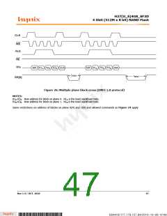
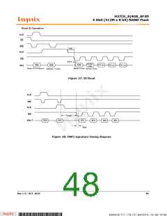
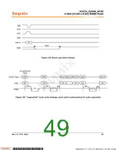
Figure 25: Multiple plane block erase (traditional protocol)
NOTE: the figure refers to x8 case. Please refer to Section 1.4 for address remapping rules for the x16 case
Rev 1.4 / OCT. 2010
46
B34416/177.179.157.84/2010-10-08 10:08
*ba53f20d-240c*

 HYNIX [ HYNIX SEMICONDUCTOR ]