APCPCWM_4828539:WP_0000001WP_0000001
1
H27(U_S)4G8_6F2D
4 Gbit (512M x 8 bit) NAND Flash
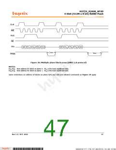
CLE
WE
ALE
RE
IOx
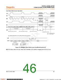
R2B R3B
R1A
R1B
D0h
60h
R2A R3A
60h
D1h
t
IEBSY
t
BERS
SR[6]
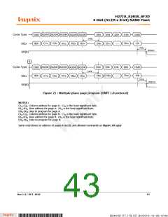
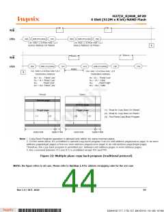
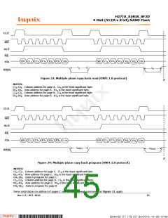
Figure 26: Multiple plane block erase (ONFI 1.0 protocol)
NOTES:
R1A-R3A Row address for block on plane 0. R1A is the least significant byte.
R1B-R3B Row address for block on plane 1. R1B is the least significant byte.
Same restrictions on address of blocks on plane 0(A) and 1(B) and allowed commands as Figure 24 apply
Rev 1.4 / OCT. 2010
47
B34416/177.179.157.84/2010-10-08 10:08
*ba53f20d-240c*

 HYNIX [ HYNIX SEMICONDUCTOR ]