APCPCWM_4828539:WP_0000001WP_0000001
1
H27(U_S)4G8_6F2D
4 Gbit (512M x 8 bit) NAND Flash
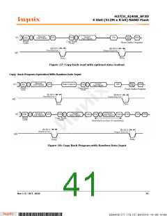
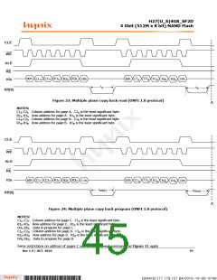
CLE
WE
ALE
RE
C2B
C1B
00h
C2A R1A
R3A
R1B
C1A
R2A
35h
R2
B
00h
R3B 35h
IOx
t
t
R
R
SR[6]
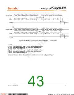
Figure 23: Multiple plane copy back read (ONFI 1.0 protocol)
A
NOTES:
C1A-C2A Column address for page A. C1A is the least significant byte.
R1A-R3A Row address for page A. R1A is the least significant byte.
C1B-C2B Column address for page B. C1B is the least significant byte.
R1B-R3B Row address for page B. R1B is the least significant byte.
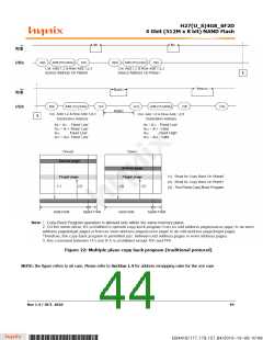
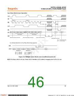
CLE
WE
ALE
RE
C2D
IOx
C1D
85h
C2C R1C
R3C
85h
R1D
C1C
R2C
11h
R2
D
R3D 10h
t
t
IPBSY
PROG
SR[6]
A
Figure 24: Multiple plane copy back program (ONFI 1.0 protocol)
NOTES:
C1C-C2C Column address for page C. C1A is the least significant byte.
R1C-R3C Row address for page C. R1A is the least significant byte.
D0C-DnC Data to program for page C.
C1D-C2D Column address for page D. C1B is the least significant byte.
R1D-R3D Row address for page D. R1B is the least significant byte.
D0D-DnD Data to program for page D.
Same restrictions on address of pages C and D, and allowed commands as Figure 21 apply
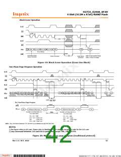
Rev 1.4 / OCT. 2010
45
B34416/177.179.157.84/2010-10-08 10:08
*ba53f20d-240c*

 HYNIX [ HYNIX SEMICONDUCTOR ]