APCPCWM_4828539:WP_0000001WP_0000001
1
H27(U_S)4G8_6F2D
4 Gbit (512M x 8 bit) NAND Flash
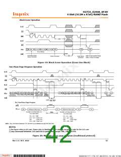
Block Erase Operation
CLE
CE
tWC
WE
tWHR
tBERS
tWB
ALE
RE
70h
Roꢆ Add1 Roꢆ Add±
Roꢆ Add3
D0h
I/O0
62ꢇ
IOx
R/B
Row Address
BUSY
Auto Block Erase
Setup Command
IO0=0 Successful Erase
IO0=1 Error in Erase
Erase Command
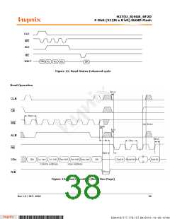
Read Status
Command
Figure 19: Block Erase Operation (Erase One Block)
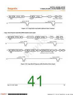
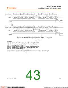
Two-Plane Page Program Operation
CLE
CE
tWC
WE
tDBSY
tWB
tWB
tPROG
tWHR
ALE
RE
tADL
tADL
Row
Add1
Row
Add3
Row
Add2
Col.
Col.
Add1
Col.
Row
Col.
Add2
Din
M
Din
M
Row
Din
N
Din
N
Row
81h
80h
11h
10h
IO
70h
Add1
Coꢄumn Address
I/Ox
Add2 Add1
Add2
Paꢅe Roꢆ Address
Add3
Proꢅram
Command
(Dummꢂ)
1 up to ±11± Bꢂte
Data Seriaꢄ Input
Seriaꢄ Data
Input Command
Program Confirm
Command (True)
Read Staus
Command
R/B
tDBSY: typ. 500us
max. 1us
Ex.) Tow-Plane Page Program
tPROG
tDBSY
R/B
IO 0~7
Address & Data Input
12ꢇ
82ꢇ
Address & Data Input
11ꢇ
81ꢇ
72ꢇ
Col Add 1,2 & Row Add 1,2,3
2112 Byte Data)
Col Add 1,2 & Row Add 1,2,3
2112 Byte Data)
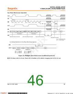
Note
A0 ~ A11 : Valid
A0 ~ A11 : Valid
A12 ~ A17 : Valid
A12 ~ A17 : Fixed ‘Low’
A18
: Fixed ‘Low’
A18
: Fixed “High’
A19 ~ A28 : Fixed ‘Low’
A19 ~ A28 : Valid
Note : Anꢂ command betꢆeen 11ꢇ and 81ꢇ is proꢇibited except 72ꢇ and FFꢇ
NOTES:
1) the figure refers to x8 case. Please refer to Section 1.4 for address remapping rules for the x16 case
2) any command between 11h and 81h is prohibited except 70h, 78h and FFh
Figure 20: Multiple plane page program (traditional protocol)
Rev 1.4 / OCT. 2010
42
B34416/177.179.157.84/2010-10-08 10:08
*ba53f20d-240c*

 HYNIX [ HYNIX SEMICONDUCTOR ]