APCPCWM_4828539:WP_0000001WP_0000001
1
H27(U_S)4G8_6F2D
4 Gbit (512M x 8 bit) NAND Flash
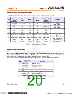
3.13 Read Status Register field definition
Table 12 below lists the meaning of each bit of Read Status Register and Read Status Enhanced
Page
Program/
Page
Cache
Program/
Cache
Block
Erase
Cache
Read
IO
Read
CODING
Reprogram
reprogram
N Page
Pass: ‘0’ Fail: ‘1’
0
1
Pass / Fail
NA
Pass / Fail
NA
NA
NA
NA
NA
Pass / Fail
Pass / Fail
N - Page
Pass: ‘0’ Fail: ‘1’
2
3
4
NA
NA
NA
NA
NA
NA
NA
NA
NA
NA
NA
NA
NA
NA
NA
-
-
-
Active: ‘0’
Idle: ‘1’
5
6
7
Ready / Busy Ready / Busy Ready / Busy Ready / Busy
Ready / Busy Ready / Busy Ready / Busy Ready / Busy
Ready / Busy
Ready / Busy
Data cache Read/Busy
Busy: ‘0’ Ready: ‘1’
Write
Write
Write
Write
Write
Protect
Protected: ‘0’
Not Protected: ‘1’
Protect
Protect
Protect
Protect
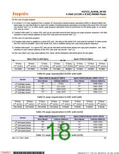
Table 12: Status Register Coding
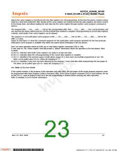
3.14 Read EDC status register
This operation is available only in copy back program and it allows the detection of errors occurred during read for copy
back. In case of multiple plane copy back, it is not possible to know which of the two read operation caused the error.
After writing Read EDC status register command (7Bh) to the command register, a read cycle outputs the content of the
EDC Register to the I/O pins on the falling edge of CE# or RE#, whichever occurs last.
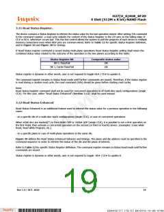
Operation is same as read status register command. Refer to Table 13 for specific EDC Register definitions:
Copy back
program
IO
CODING
0
1
2
3
4
5
6
7
Pass / Fail
Pass: ‘0’ Fail: ‘1’
EDC status
EDC validity
NA
No error: ‘0’ Error: ‘1’
Invalid: ‘0’ Valid: ‘1’
-
NA
-
Ready / Busy
Ready / Busy
Write Protect
Busy: ‘0’ Ready: ‘1’
Busy: ‘0’ Ready: ‘1’
Protected: ‘0’ Not Protected: ‘1’
Table 13: EDC register coding
Rev 1.4 / OCT. 2010
20
B34416/177.179.157.84/2010-10-08 10:08
*ba53f20d-240c*

 HYNIX [ HYNIX SEMICONDUCTOR ]