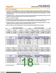
APCPCWM_4828539:WP_0000001WP_0000001
1
H27(U_S)4G8_6F2D
4 Gbit (512M x 8 bit) NAND Flash
3.17 Cache Program
Cache Program is used to improve the program throughput by programing data using the cache register. The cache pro-
gram operation can only be used within one block. The cache register allows new data to be input while the previous data
that was transffered to the page buffer is programmed into the memory array.
Cache program is available only within a block
After the serial data input command (80h) is loaded to the command register, followed by 5 cycles of address, a full or
partial page of data is latched into the cache register.
Once the cache write command (15h) is loaded to the command register, the data in the cache register is transferred into
the data register for cell programming. At this time the device remains in Busy state For a short time (tCBSYW). After all
data of the cache register are transferred into the data register, the device returns to the Ready state, and allows loading
the next data into the cache register through another cache program command sequence (80h-15h).
The Busy time following the first sequence 80h - 15h equals the time needed to transfer the data of cache register to the
data register. Cell programming of the data of data register and loading of the next data into the cache register is conse
quently processed through a pipeline model.
In case of any subsequent sequence 80h - 15h, transfer from the cache register to the data register is held off until cell
programming of current data register contents is complete: till this moment the device will stay in a busy state (tCBSYW).
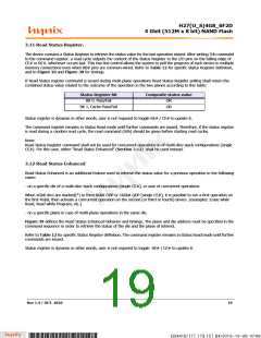
Read Status commands (70h or 78h) may be issued to check the status of the different registers, and the pass/fail status
of the cached program operations. More in detail:
a) the Cache-Busy status bit I/O<6> indicates when the cache register is ready to accept new data.
b) the status bit I/O<5> can be used to determine when the cell programming of the current data register contents is
complete.
c) the cache program error bit I/O<1> can be used to identify if the previous page (page N-1) has been successfully
programmed or not in cache program operation. The latter can be polled upon I/O<6> status bit changing to "1" .
d) the error bit I/O<0> is used to identify if any error has been detected by the program / erase controller while program
ming page N. The latter can be polled upon I/O<5> status bit changing to "1".
I/O<1> may be read together with I/O<0>.
If the system monitors the progress of the operation only with R/B#, the last page of the target program sequence must
be programmed with Page Program Confirm command (10h). If the Cache Program command (15h) is used instead, the
status bit I/O<5> must be polled to find out if the last programming is finished before starting any other operation.
See Table 12 and Figure 40 for more details.
3.18 Multi-plane Cache Program
The device supports multi-plane cache program, which enables high program throughput by programming two pages in
parallel while exploiting the data and cache registers of both planes to implement cache.
The device supports both the traditional and ONFI 1.0 command sets.
The command sequence can be summarized as follows:
a) Serial Data Input command (80h), followed by the five cycle address inputs and then serial data for the 1st page. Ad
dress for this page must be within 1st plane (A<20>=0). The data of 1st page other than those to be programmed do
not need to be loaded. The device supports random data input exactly like page program operation.
b) The Dummy Page Program Confirm command (11h) stops 1st page data input and the device becomes busy for a short
time (tDBSY).
c) Once device returns to ready again, 81h (or 80h) command must be issued, followed by 2nd page address (5 cycles)
and its serial data input. Address for this page must be within 2nd plane (A<20>=1). The data of 2nd page other than
those to be programmed do not need to be loaded.
d) Cache Program confirm command (15h) Once the cache write command (15h) is loaded to the command register, the
Rev 1.4 / OCT. 2010
22
B34416/177.179.157.84/2010-10-08 10:08
*ba53f20d-240c*

 HYNIX [ HYNIX SEMICONDUCTOR ]