APCPCWM_4828539:WP_0000001WP_0000001
1
H27(U_S)4G8_6F2D
4 Gbit (512M x 8 bit) NAND Flash
For the case of page program
1) In section 3.2 it was explained that a number of consecutive partial program operations (NOP) is allowed within the
same page. In case this feature is used, the number of partial program operations occurring in the same EDC unit must
not exceed "one" (1). In other words, page program operations must be performed on the whole page, or on whole
EDC unit at a time.
2) "random data input" in a given EDC unit can be executed several times during one page program sequence, but data
insertion in each column address of each EDC unit must not exceed "one" (1).
For the case of copy back program
1) If random data input is applied in a given EDC unit, the data of the whole EDC unit must be inserted. In other words,
the EDC check is possible only if the whole EDC unit is modified during one copy back program sequence
2) "random data input" in a given EDC unit can be executed several times during one copy back sequence , but data
insertion in each column address of the EDC unit must not exceed "one" (1)
For the user which use Copy Back without EDC check, all the limitations described above do not apply.
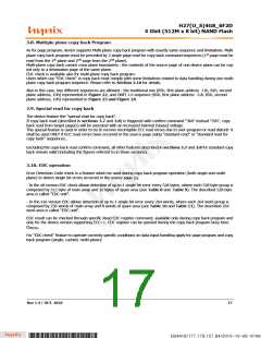
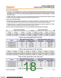
Main Field (2,048 Byte)
Spare Field (64 Byte)
“A”area
“B”area
“C”area
“D”area
“E”area
(1st sector) (2nd sector) (3rd sector) (4th sector)
16 Byte 16 Byte 16 Byte 16 Byte
“F”area
“G”area
“H”area
(1st sector)
(2nd sector)
(3rd sector)
(4th sector)
512 Byte
512 Byte
512 Byte
512 Byte
Table 8: page organization in EDC units (x8)
Main Field (Column 0~2047) Spare Field (Column 2048~2111)
Sector
Area Name
Column Address
0~511
Area Name
Column Address
2048~2063
1st 528-Byte Sector
nd 528-Byte Sector
rd 528-Byte Sector
th 528-Byte Sector
“A”
“B”
“C”
“D”
“E”
“F”
“G”
“H”
512~1023
2064~2079
2
1024~1535
1536~2047
2080~2095
3
4
2096~2111
Table 9: page organization in EDC units (x8)
“A”area
(1st sector)
“B”area
(2nd sector)
“C”area
(3rd sector)
“D”area
(4th sector)
“E”area
(1st sector)
“F”area
(2nd sector)
“G”area
“H”area
(3rd sector) (4th sector)
256 words
256 words
256 words
256 words
8 words
8 words
8 words
8 words
Table 10: page organization in EDC units (x16)
Main Field (Column 0~1023) Spare Field (Column 1024~1055)
Sector
Area Name
Column Address
0~255
Area Name
Column Address
1024~1031
1st 264-word Sector
nd 264-word Sector
rd 264-word Sector
th 264-word Sector
“A”
“B”
“C”
“D”
“E”
“F”
“G”
“H”
256~511
1032~1039
2
512~767
1040~1047
3
4
768~1023
1048~1055
Table 11: page organization in EDC units (x16)
Rev 1.4 / OCT. 2010
18
B34416/177.179.157.84/2010-10-08 10:08
*ba53f20d-240c*

 HYNIX [ HYNIX SEMICONDUCTOR ]