APCPCWM_4828539:WP_0000001WP_0000001
1
H27(U_S)4G8_6F2D
4 Gbit (512M x 8 bit) NAND Flash
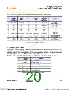
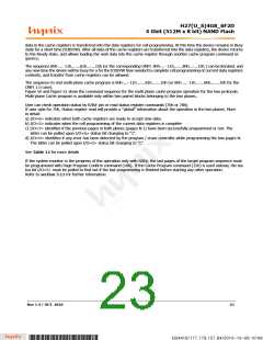
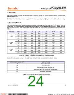
3.19 Read ID.
The device contains a product identification mode, initiated by writing 90h to the command register, followed by an
address input of 00h.
The 5-byte Read ID configuration are supported: The device operating mode (5-byte) is selected through cam setting.
3.19.1 Legacy Read ID
Five read cycles sequentially output the manufacturer code (20h), and the device code and 3rd, 4th, and 5th cycle ID,
respectively. The command register remains in Read ID mode until further commands are issued to it. Figure 27 shows
the operation sequence, while Table 14 to Table 18 explain the byte meaning. Complete read id code table is as
follows.
1st
2nd
DCh
CCh
ACh
BCh
D3h
C3h
A3h
B3h
D5h
C5h
A5h
B5h
3rd
90h
90h
90h
90h
D1h
D1h
D1h
D1h
D2h
D2h
D2h
D2h
4th (1)
95h
D5h
15h
55h
95h
D5h
15h
55h
95h
D5h
15h
55h
5th
54h
54h
54h
54h
58h
58h
58h
58h
5Ch
5Ch
5Ch
5Ch
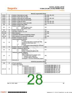
DENSITY
ORG
X8
VCC
3.0V
3.0V
1.8V
1.8V
3.0V
3.0V
1.8V
1.8V
3.0V
3.0V
1.8V
1.8V
ADh
ADh
ADh
ADh
ADh
ADh
ADh
ADh
ADh
ADh
ADh
ADh
X16
X8
4 Gbit
X16
X8
X16
X8
8 Gbit
DDP
X16
X8
X16
X8
16 Gbit
QDP
X16
Table 14: Legacy " Read ID for supported configurations
NOTE: for 1.8V version, IO<7,3>=00 would mean "50nsec", while device serial cycle time is 45nsec
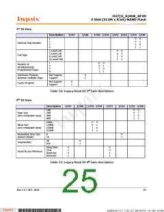
DEVICE IDENTIFIER BYTE
DESCRIPTION
Manufacturer Code
1st
2nd
3rd
4th
5th
Device Identifier
Internal chip number, cell type, etc.
Page Size, Block Size, Spare Size, Organization
Multiplane information
Table 15: "Legacy" Read ID bytes meaning
Rev 1.4 / OCT. 2010
24
B34416/177.179.157.84/2010-10-08 10:08
*ba53f20d-240c*

 HYNIX [ HYNIX SEMICONDUCTOR ]