APCPCWM_4828539:WP_0000001WP_0000001
1
H27(U_S)4G8_6F2D
4 Gbit (512M x 8 bit) NAND Flash
data in the cache registers is transferred into the data registers for cell programming. At this time the device remains in Busy
state for a short time (tCBSYW). After all data of the cache registers are transferred into the data registers, the device returns
to the Ready state, and allows loading the next data into the cache register through another cache program command se
quence.
The sequence 80h-...- 11h...-...81h...-...15h (or the corresponding ONFI 80h-...- 11h...-...80h...-...15h ) can be iterated, and
any new time the device will be busy for a for the tCBSYW time needed to complete cell programming of current data registers
contents, and transfer from cache registers can be allowed.
The sequence to end multi-plane cache program is 80h-...- 11h...-...81h...-...10h (or 80h-...- 11h...-...80h...-...10h for the
ONFI 1.0 case).
Figure 50 and Figure 51 show the command sequence for the multi plane cache program operation for the two protocols.
Multi-plane Cache program is available only within two paired blocks belonging to the two planes..
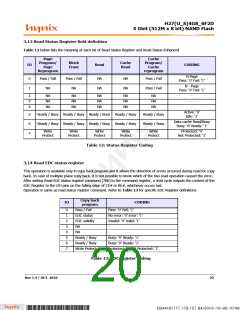
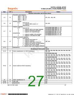
User can check operation status by R/B# pin or read status register commands (70h or 78h)
If user opts for 70h, Status register read will provide a "global" information about the operation in the two planes. More
in detail:
a) I/O<6> indicates when both cache registers are ready to accept new data.
b) I/O<5> indicates when the cell programming of the current data registers is complete
c) I/O<1> identifies if the previous pages in both planes (pages N-1) have been successfully programmed or not. The
latter can be polled upon I/O<6> status bit changing to "1".
d) I/O<0> identifies if any error has been detected by the program / erase controller while programming the two pages N.
The latter can be polled upon I/O<5> status bit changing to "1".
See Table 12 for more details
If the system monitor rs the progress of the operation only with R/B#, the last pages of the target program sequence must
be programmed with Page Program Confirm command (10h). If the Cache Program command (15h) is used instead, the sta
tus bit I/O<5> must be polled to find out if the last programming is finished before starting any other operation.
Refer to section 3.11 for further information.
Rev 1.4 / OCT. 2010
23
B34416/177.179.157.84/2010-10-08 10:08
*ba53f20d-240c*

 HYNIX [ HYNIX SEMICONDUCTOR ]