HT46R01A
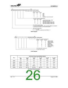
The following timing diagram shows graphically the various stages involved in an analog to digital conversion process
and its associated timing.
S
T
A
R
T
b
i
t
s
e
t
h
i
g
h
w
i
t
h
i
n
o
n
e
t
o
t
e
n
i
n
s
t
r
u
c
t
i
o
n
c
y
c
l
e
s
a
f
t
e
r
t
h
e
P
C
R
0
~
P
C
R
2
b
i
t
s
c
h
a
n
g
e
s
t
a
t
e
S
T
A
R
T
A
/
D
s
a
m
p
l
i
n
g
t
i
m
e
A
/
D
s
a
m
p
l
i
n
g
t
i
m
e
A
/
D
s
a
m
p
l
i
n
g
t
i
m
e
E
O
C
B
3
2
t
A
D
3
2
t
A
D
3
2
t
P
C
R
2
~
0
0
0
B
0
1
1
B
1
0
0
B
0
0
0
B
P
C
R
0
1
.
P
A
t
B
p
o
r
t
s
e
t
u
p
a
s
I
/
O
s
2
.
/
D
c
o
n
v
e
r
t
e
r
i
s
p
o
w
e
r
e
d
o
f
f
o
r
e
d
u
c
e
p
o
w
e
r
c
o
n
s
u
m
p
t
i
o
n
A
C
S
2
~
0
0
0
B
0
1
0
B
0
0
0
B
0
0
1
B
D
o
n
'
t
c
a
r
e
A
C
S
0
P
o
w
e
r
-
o
n
S
t
a
r
t
o
f
A
/
D
S
t
a
r
t
o
f
A
/
D
S
t
a
r
t
o
f
A
/
D
R
e
s
e
t
c
o
n
v
e
r
s
i
o
n
c
o
n
v
e
r
s
i
o
n
c
o
n
v
e
r
s
i
o
n
R
e
s
e
t
A
/
D
R
e
s
e
t
A
/
D
R
e
s
e
t
A
/
D
c
o
n
v
e
r
t
e
r
c
o
n
v
e
r
t
e
r
c
o
n
v
e
r
t
e
r
E
n
d
o
f
A
/
D
E
n
d
o
f
A
/
D
E
n
d
o
f
A
/
D
c
o
n
v
e
r
s
i
o
n
c
o
n
v
e
r
s
i
o
n
c
o
n
v
e
r
s
i
o
n
1
:
D
e
f
i
n
e
P
B
c
o
n
f
i
g
u
r
a
t
i
o
n
2
:
S
e
l
e
c
t
a
n
a
l
o
g
c
h
a
n
n
e
l
t
A
D
C
t
A
D
C
t
A D C
A
/
D
c
o
n
v
e
r
s
i
o
n
t
i
m
e
A
/
D
c
o
n
v
e
r
s
i
o
n
t
i
m
e
A
/
D
c
o
n
v
e
r
s
i
o
n
t
i
m
e
N
o
t
e
:
S
Y
S
S
Y
S
S
Y
S
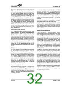
A/D Conversion Timing
The setting up and operation of the A/D converter func-
tion is fully under the control of the application program
as there are no configuration options associated with
the A/D converter. After an A/D conversion process has
been initiated by the application program, the
microcontroller internal hardware will begin to carry out
the conversion, during which time the program can con-
tinue with other functions. The time taken for the A/D
conversion is dependent upon the device chosen and is
a function of the A/D clock period tAD as shown in the ta-
ble.
supplied to the internal A/D circuitry will be reduced re-
sulting in a reduction of supply current. This ability to re-
duce power by turning off the internal A/D function by
clearing the A/D channel selection bits may be an impor-
tant consideration in battery powered applications.
Another important programming consideration is that
when the A/D channel selection bits change value the
A/D converter must be re-initialised. This is achieved by
pulsing the START bit in the ADCR register immediately
after the channel selection bits have changed state. The
exception to this is where the channel selection bits are
all cleared, in which case the A/D converter is not re-
quired to be re-initialised.
Device
A/D Conversion Time
HT46R01A
64tAD
A/D Programming Example
A/D Conversion Time
The following two programming examples illustrate how
to setup and implement an A/D conversion. In the first
example, the method of polling the EOCB bit in the
ADCR register is used to detect when the conversion
cycle is complete, whereas in the second example, the
A/D interrupt is used to determine when the conversion
is complete.
Programming Considerations
When programming, special attention must be given to
the A/D channel selection bits in the ADCR register. If
these bits are all cleared to zero no external pins will be
selected for use as A/D input pins allowing the pins to be
used as normal I/O pins. When this happens the power
Example: using an EOCB polling method to detect the end of conversion.
clr
mov
mov
EADI
a,00000001B
ACSR,a
; disable ADC interrupt
; setup the ACSR register to select fSYS/8 as
; the A/D clock
mov
mov
a,00100000B
; setup ADCR register to configure Port PA0~PA3
; as A/D inputs
; and select AN0 to be connected to the A/D
; converter
ADCR,a
:
Rev. 1.10
28
August 13, 2008

 HOLTIC [ HOLT INTEGRATED CIRCUITS ]