HT46R01A
·
·
A/D Input Pins
Step 1
Select the required A/D conversion clock by correctly
programming bits ADCS0 to ADCS20 in the ACSR
register.
All of the A/D analog input pins are pin-shared with the
I/O pins on Port A. Bits PCR0~PCR2 in the ADCR regis-
ter, not configuration options, determine whether the in-
put pins are setup as normal Port A input/output pins or
whether they are setup as analog inputs. In this way,
pins can be changed under program control to change
their function from normal I/O operation to analog inputs
and vice versa. Pull-high resistors, which are setup via
the PAPU register, apply to the input pins only when they
are used as normal I/O pins, if setup as A/D inputs the
pull-high resistors will be automatically disconnected.
Note that it is not necessary to first setup the A/D pin as
an input in the PAC port control register to enable the
A/D input, when the PCR2~PCR0 bits enable an A/D in-
put, the status of the port control register will be overrid-
den. The VDD power supply pin is used as the A/D
converter reference voltage, and as such analog inputs
must not be allowed to exceed this value. Appropriate
measures should also be taken to ensure that the VDD
pin remains as stable and noise free as possible.
Step 2
Select which pins on Port A are to be used as A/D in-
puts and configure them as A/D input pins by correctly
programming the PCR0~PCR2 bits in the ADCR reg-
ister.
·
Step 3
Select which channel is to be connected to the internal
A/D converter by correctly programming the
ACS0~ACS2 bits which are also contained in the
ADCR register. Note that this step can be combined
with Step 2 into a single ADCR register programming
operation.
·
Step 4
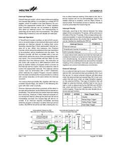
If the interrupts are to be used, the interrupt control
registers must be correctly configured to ensure the
A/D converter interrupt function is active. The master
interrupt control bit, EMI, in the interrupt control regis-
ter must be set high and the A/D converter interrupt
bit, EADI, in the interrupt control register must also be
set high.
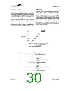
Initialising the A/D Converter
The internal A/D converter must be initialised in a spe-
cial way. Each time the A/D channel selection bits are
modified by the program, the A/D converter must be
re-initialised. If the A/D converter is not initialised after
the channel selection bits are changed, the EOCB flag
may have an undefined value, which may produce a
false end of conversion signal. To initialise the A/D con-
verter after the channel selection bits have changed,
then, within a time frame of one to ten instruction cycles,
the START bit in the ADCR register must first be set high
and then immediately cleared to zero. This will ensure
that the EOCB flag is correctly set to a high condition.
·
·
Step 5
The analog to digital conversion process can now be
initialised by setting the START bit in the ADCR regis-
ter from low to high and then low again. Note that this
bit should have been originally set to a zero value.
Step 6
To check when the analog to digital conversion pro-
cess is complete, the EOCB bit in the ADCR register
can be polled. The conversion process is complete
when this bit goes low. When this occurs the A/D data
registers be read to obtain the conversion value. As
an alternative method if the interrupts are enabled and
the stack is not full, the program can wait for an A/D in-
terrupt to occur.
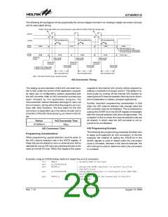
Summary of A/D Conversion Steps
Note: When checking for the end of the conversion
process, if the method of polling the EOCB bit in
the ADCR register is used, the interrupt enable
step above can be omitted.
The following summarises the individual steps that
should be executed in order to implement an A/D con-
version process.
Rev. 1.10
27
August 13, 2008

 HOLTIC [ HOLT INTEGRATED CIRCUITS ]