HT46R01A
The START bit in the ADCR register is used to start and
reset the A/D converter. When the microcontroller sets
this bit from low to high and then low again, an analog to
digital conversion cycle will be initiated. When the
START bit is brought from low to high but not low again,
the EOCB bit in the ADCR register will be set high and
the analog to digital converter will be reset. It is the
START bit that is used to control the overall on/off opera-
tion of the internal analog to digital converter.
A/D Converter Data Registers - ADR
As the device has an 8-bit A/D converter, a single regis-
ter, known as ADR, is used to store the 8-bit analog to
digital conversion value. After the conversion process
takes place, this register can be directly read by the
microcontroller to obtain the digitised conversion value.
In the following tables, D0~D7 are the A/D conversion
data result bits.
The EOCB bit in the ADCR register is used to indicate
when the analog to digital conversion process is com-
plete. This bit will be automatically cleared to zero by the
microcontroller after a conversion cycle has ended. In
addition, the corresponding A/D interrupt request flag
will be set in the interrupt control register, and if the inter-
rupts are enabled, an appropriate internal interrupt sig-
nal will be generated. This A/D internal interrupt signal
will direct the program flow to the associated A/D inter-
nal interrupt address for processing. If the A/D internal
interrupt is disabled, the microcontroller can be used to
poll the EOCB bit in the ADCR register to check whether
it has been cleared as an alternative method of detect-
ing the end of an A/D conversion cycle.
Register Bit7 Bit6 Bit5 Bit4 Bit3 Bit2 Bit1 Bit0
ADR
D7
D6
D5
D4
D3
D2
D1
D0
A/D Data Register
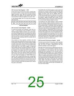
A/D Converter Control Register - ADCR
To control the function and operation of the A/D con-
verter, a control register known as ADCR is provided.
This 8-bit register defines functions such as the selec-
tion of which analog channel is connected to the internal
A/D converter, which pins are used as analog inputs and
which are used as normal I/Os as well as controlling the
start function and monitoring the A/D converter end of
conversion status.
One section of this register contains the bits
ACS2~ACS0 which define the channel number. As each
of the devices contains only one actual analog to digital
converter circuit, each of the individual 4 analog inputs
must be routed to the converter. It is the function of the
ACS2~ACS0 bits in the ADCR register to determine
which analog channel is actually connected to the inter-
nal A/D converter. Note that the ACS2 bit must always
be assigned a zero value. The ADCR control register
also contains the PCR2~PCR0 bits which determine
which pins on Port A are used as analog inputs for the
A/D converter and which pins are to be used as normal
I/O pins. If the 3-bit address on PCR2~PCR0 has a
value of ²100² or higher, then all four pins, namely AN0,
AN1, AN2 and AN3 will all be set as analog inputs. Note
that if the PCR2~PCR0 bits are all set to zero, then all
the Port B pins will be setup as normal I/Os and the inter-
nal A/D converter circuitry will be powered off to reduce
the power consumption.
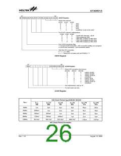
A/D Converter Clock Source Register - ACSR
The clock source for the A/D converter, which originates
from the system clock fSYS, is first divided by a division
ratio, the value of which is determined by the bits
ADCS0 to ADCS2 in the ACSR register.
Although the A/D clock source is determined by the sys-
tem clock fSYS, and by bits ADCS0 to ADCS2, there are
some limitations on the maximum A/D clock source
speed that can be selected. As the minimum value of
permissible A/D clock period, tAD, is 1us for all devices,
care must be taken for system clock speeds in excess of
1MHz. For system clock speeds in excess of 1MHz, the
ADCS0 to ADCS2 bits should not be set to give an A/D
clock period less than the specified minimum A/D clock
period which may result in inaccurate A/D conversion
values. Refer to the table for examples, where values
marked with an asterisk * show where special care must
be taken, as the values are less than the specified mini-
mum A/D Clock Period.
Rev. 1.10
25
August 13, 2008

 HOLTIC [ HOLT INTEGRATED CIRCUITS ]