HT46R01A
PWM Output Control
Analog to Digital Converter
The PWM output is pin-shared with the I/O pin PA4. To
operate as a PWM output and not as an I/O pin, the cor-
rect bits must be set in the CTRL0 register. A zero value
must also be written to the corresponding bit in the I/O
port control register PAC.4 to ensure that the PWM out-
put pin is setup as an output. After these two initial steps
have been carried out, and of course after the required
PWM value has been written into the PWM register, writ-
ing a high value to the corresponding bit in the output
data register PA.4 will enable the PWM data to appear
on the pin. Writing a zero value will disable the PWM
output function and force the output low. In this way, the
Port A data output register can be used as an on/off con-
trol for the PWM function. Note that if the CTRL0 register
has selected the PWM function, but a high value has
been written to its corresponding bit in the PAC control
register to configure the pin as an input, then the pin can
still function as a normal input line, with pull-high resistor
options.
The need to interface to real world analog signals is a
common requirement for many electronic systems.
However, to properly process these signals by a
microcontroller, they must first be converted into digital
signals by A/D converters. By integrating the A/D con-
version electronic circuitry into the microcontroller, the
need for external components is reduced significantly
with the corresponding follow-on benefits of lower costs
and reduced component space requirements.
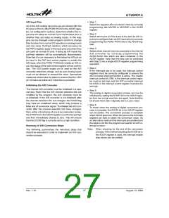
A/D Overview
The device contains a 4-channel analog to digital con-
verter which can directly interface to external analog sig-
nals, such as that from sensors or other control signals
and convert these signals directly into an 8-bit digital
value.
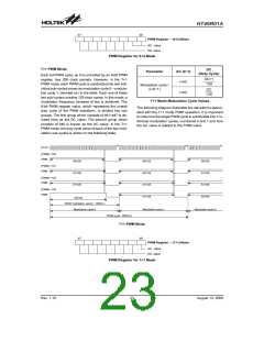
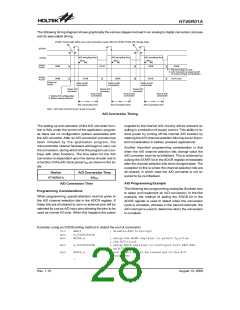
The following diagram shows the overall internal struc-
ture of the A/D converter, together with its associated
registers.
PWM Programming Example
The following sample program shows how the PWM
output is setup and controlled.
mov a,64h
; setup PWM value of 100
; decimal which is 64H
mov pwm,a
set ctrl.5 ; select the 7+1 PWM mode
set ctrl.3 ; select pin PA4 to have a PWM
; function
clr pac.4
set pa.4
; setup pin PA4 as an output
; PD.0=1; enable the PWM
; output
:
:
clr pa.4
; disable the PWM output - pin
; PD4 forced low
C
l
o
c
k
D
i
v
i
d
e
R
a
t
i
o
A
D
C
S
o
u
r
c
e
¸
A
C
S
R
R
e
g
i
s
t
e
r
N
S
Y
S
V
D
D
A
/
D
r
e
f
e
r
e
n
c
e
v
o
l
t
a
g
e
P
P
A
A
0
1
/
/
A
A
N
N
0
1
A
/
D
D
a
t
a
A
D
C
A
D
R
P
A
2
/
A
N
2
R
e
g
i
s
t
e
r
s
P
A
3
/
A
N
3
A
D
C
R
P
C
R
0
~
P
C
R
2
A
D
C
S
0
~
A
D
C
S
2
S
T
A
R
T
E
O
C
R
e
g
i
s
t
e
r
P
i
n
C
o
n
f
i
g
u
r
a
t
i
o
n
C
h
a
n
n
e
l
S
e
l
e
c
t
S
t
a
r
t
a
n
d
E
n
d
o
f
B
i
t
s
B
i
t
s
C
o
n
v
e
r
s
i
o
n
B
i
t
s
A/D Converter Structure
Rev. 1.10
24
August 13, 2008

 HOLTIC [ HOLT INTEGRATED CIRCUITS ]