HT46RU66/HT46CU66
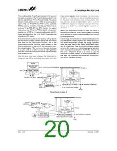
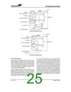
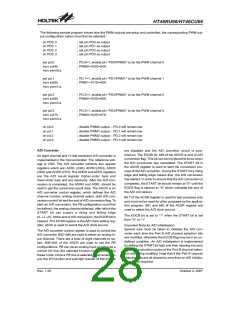
Port PB can also be used as A/D converter inputs. There is a PWM function shared with PD0/PD1/PD2/PD3. If the
PWM function is enabled, the PWM0/PWM1/PWM2/ PWM3 signal will appear on PD0/PD1/PD2/PD3, if PD0/ PD1/
PD2/PD3 are operating in output mode. Writing ²1² to the PD0~PD3 data register will enable the PWM output function
while writing ²0² will force the PD0~PD3 to remain at ²0². The I/O functions of the PD0/PD1/PD2/PD3 are shown below.
I/O Mode
I/P (Normal)
O/P (Normal)
I/P (PWM)
O/P (PWM)
PD0~PD3
Logical Input
Logical Output
Logical Input
PWM0~PWM3
It is recommended that unused or not bonded out I/O lines should be set as output pins by software instruction to avoid
consuming power under input floating state.
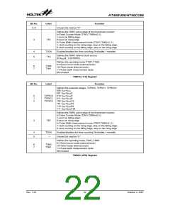
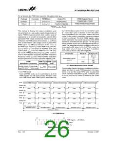
The definitions of the PFD control signal and PFD output frequency are listed in the following table.
Timer
OFF
OFF
ON
Timer Preload Value
PA3 Data Register
PA3 Pad State
PFD Frequency
X
X
N
N
0
1
0
1
0
U
X
X
0
X
ON
PFD
fTMR/[2´(M-N)]
Note:
²X² stands for unused
²U² stands for unknown
²M² is ²65536² for PFD0 or PFD1
²N² is the preload value for the timer/event counter
²fTMR² is input clock frequency for timer/event counter
V
D
D
P
u
l
l
-
h
i
g
h
C
o
n
t
r
o
l
B
i
t
O
p
t
i
o
n
P
P
A
A
0
1
/
/
B
B
Z
Z
D
a
t
a
B
u
s
D
Q
W
r
i
t
e
C
o
n
t
r
o
l
R
e
g
i
s
t
e
r
C
K
Q
P
A
2
P
A
3
/
~
P
F
D
S
P
A
4
P
A
7
C
h
i
p
R
e
s
e
t
P
B
0
/
A
N
M
0
~
P
B
7
/
A
N
7
P
C
0
/
T
R
2
R
e
a
d
C
o
n
t
r
o
l
R
e
g
i
s
t
e
r
P
C
1
~
P
C
5
D
a
t
a
B
i
t
P
D
0
/
P
W
W
W
W
M
0
1
2
3
P
D
1
/
P
M
D
Q
P
D
2
/
P
M
W
r
i
t
e
D
a
t
a
R
e
g
i
s
t
e
r
C
K
Q
P
D
3
/
P
M
S
P
D
4
/
I
N
T
0
1
P
D
5
6
7
/
/
/
I
T
T
N
T
P
D
M
M
R
R
0
1
M
U
P
D
P
A
0
/
P
A
1
/
P
A
3
/
P
D
0
/
P
D
1
/
P
D
2
/
P
D
3
X
B
Z
/
B
Z
/
P
F
D
/
P
W
M
0
/
P
W
M
1
/
P
W
M
2
/
P
W
M
3
M
E
N
U
X
R
e
a
d
D
a
t
a
R
e
g
i
s
t
e
r
S
y
s
t
e
m
W
a
k
e
-
u
p
W
a
k
e
-
u
p
O
p
t
i
o
n
s
(
P
A
o
n
l
y
)
I
N
T
T
0
f
o
r
P
D
4
o
n
l
y
I
N
1
f
o
r
P
D
5
o
n
l
y
T
M
R
0
f
f
o
o
r
r
P
P
D
6
o
o
n
n
l
l
y
y
T
M
R
1
D
7
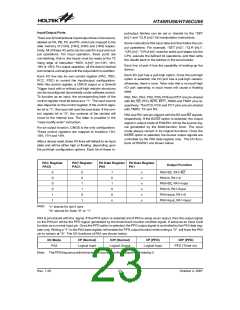
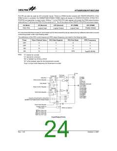
Input/Output Ports
Rev. 1.20
24
October 2, 2007

 HOLTEK [ HOLTEK SEMICONDUCTOR INC ]