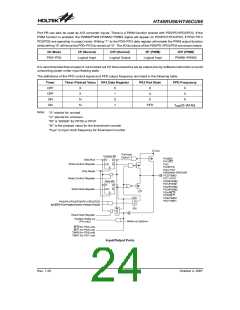
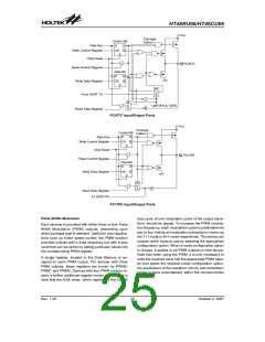
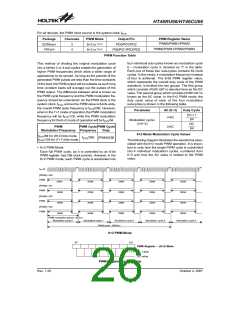
HT46RU66/HT46CU66
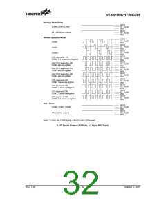
The following sample program shows how the PWM outputs are setup and controlled, the corresponding PWM out-
put configuration option must first be selected.
clr PDC.0
clr PDC.1
clr PDC.2
clr PDC.3
; set pin PD0 as output
; set pin PD1 as output
; set pin PD2 as output
; set pin PD3 as output
set pd.0
; PD.0=1; enable pin ²PD0/PWM0² to be the PWM channel 0
mov a,64h
mov pwm0,a
; PWM0=100D=64H
set pd.1
; PD.1=1; enable pin ²PD1/PWM1² to be the PWM channel 1
mov a,65h
mov pwm1,a
; PWM1=101D=65H
set pd.2
; PD.2=1; enable pin ²PD2/PWM2² to be the PWM channel 2
mov a,66h
mov pwm2,a
; PWM2=102D=66H
set pd.3
; PD.3=1; enable pin ²PD3/PWM3² to be the PWM channel 3
mov a,67h
mov pwm3,a
; PWM3=103D=67H
clr pd.0
clr pd.1
clr pd.2
clr pd.3
; disable PWM0 output - PD.0 will remain low
; disable PWM1 output - PD.1 will remain low
; disable PWM2 output - PD.2 will remain low
; disable PWM3 output - PD.3 will remain low
A/D Converter
are disabled and the A/D converter circuit is pow-
ered-on. The EOCB bit, bit6 of the ADCR is end of A/D
conversion flag. This bit can be monitored to know when
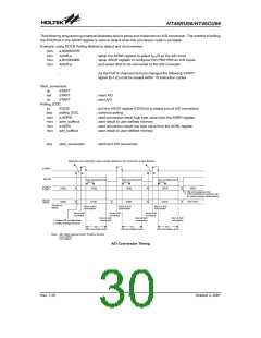
the A/D conversion has completed. The START bit in
the ADCR register is used to start the conversion pro-
cess of the A/D converter. Giving the START bit a rising
edge and falling edge means that the A/D conversion
has started. In order to ensure that the A/D conversion is
completed, the START bit should remain at ²0² until the
EOCB flag is cleared to ²0² which indicates the end of
the A/D conversion.
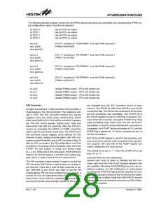
An eight channel and 12 bits resolution A/D converter is
implemented in the microcontroller. The reference volt-
age is VDD. The A/D converter contains four special
registers which are; ADRL (24H), ADRH (25H), ADCR
(26H) and ACSR (27H). The ADRH and ADRL registers
are the A/D result register higher-order byte and
lower-order byte and are read-only. After the A/D con-
version is completed, the ADRH and ADRL should be
read to get the conversion result data. The ADCR is an
A/D converter control register, which defines the A/D
channel number, analog channel select, start A/D con-
version control bit and the end of A/D conversion flag. To
start an A/D conversion, the PB configuration must first
be defined, the analog channel selected, after which the
START bit can supply a rising and falling edge
(0®1®0). At the end of A/D conversion, the EOCB bit is
cleared. The ACSR register is the A/D clock setting reg-
ister, which is used to select the A/D clock source.
Bit 7 of the ACSR register is used for test purposes only
and must not be used for other purposes by the applica-
tion program. Bit1 and bit0 of the ACSR register are
used to select the A/D clock source.
The EOCB bit is set to ²1² when the START bit is set
from ²0² to ²1².
Important Note for A/D initialisation:
Special care must be taken to initialise the A/D con-
verter each time the Port B A/D channel selection bits
are modified, otherwise the EOCB flag may be in an un-
defined condition. An A/D initialisation is implemented
by setting the START bit high and then clearing it to zero
within 10 instruction cycles of the Port B channel selec-
tion bits being modified. Note that if the Port B channel
selection bits are all cleared to zero then an A/D initialis-
ation is not required.
The A/D converter control register is used to control the
A/D converter. Bit2~bit0 are used to select an analog in-
put channel. There are a total of eight channels to se-
lect. Bit5~bit3 of the ADCR are used to set the PB
configurations. PB can be an analog input or setup as a
normal I/O line, the selected function is determined by
these 3 bits. Once a PB line is selected as an analog in-
put, the I/O function and pull-high resistor of this I/O line
Rev. 1.20
28
October 2, 2007

 HOLTEK [ HOLTEK SEMICONDUCTOR INC ]