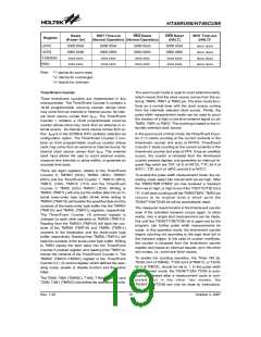
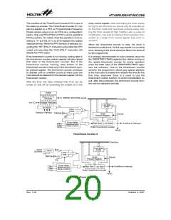
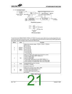
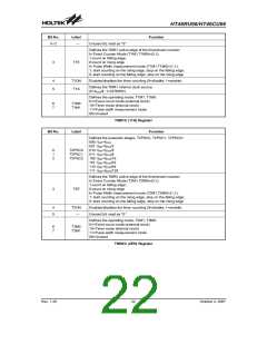
HT46RU66/HT46CU66
Input/Output Ports
put/output latches can be set or cleared by the ²SET
[m].i² and ²CLR [m].i² bit manipulation instructions.
There are 32 bidirectional input/output lines in the device,
labeled as PA, PB, PC and PD, which are mapped to the
data memory of [12H], [14H], [16H] and [18H] respec-
tively. All of these I/O ports can be used for input and out-
put operations. For input operation, these ports are
non-latching, that is, the inputs must be ready at the T2
rising edge of instruction ²MOV A,[m]² (m=12H, 14H,
16H or 18H). For output operation, all the data is latched
and remains unchanged until the output latch is rewritten.
Some instructions first input data and then follow the out-
put operations. For example, ²SET [m].i², ²CLR [m].i²,
²CPL [m]², ²CPLA [m]² read the entire port states into the
CPU, execute the defined bit operations, and then write
the results back to the latches or the accumulator.
Each line of port A has the capability of waking-up the
device.
Each I/O port has a pull-high option. Once the pull-high
option is selected, the I/O port has a pull-high resistor,
otherwise, there¢s none. Take note that a non-pull-high
I/O port operating in input mode will cause a floating
state.
Each I/O line has its own control register (PAC, PBC,
PCC, PDC) to control the input/output configuration.
With this control register, a CMOS output or a Schmitt
Trigger input with or without pull-high resistor structures
can be reconfigured dynamically under software control.
To function as an input, the corresponding latch of the
control register must be setup as a ²1². The input source
also depends on the control register. If the control regis-
ter bit is ²1², the input will read the pad state. If the con-
trol register bit is ²0², the contents of the latches will
move to the internal bus. The latter is possible in the
²read-modify-write² instruction.
PA0, PA1, PA3, PD4, PD5, PD6 and PD7 are pin-shared
with BZ, BZ, PFD, INT0, INT1, TMR0 and TMR1 pins re-
spectively. The PC0, PC6 and PC7 pins are pin-shared
with TMR2, TX and RX.
PA0 and PA1 are pin-shared with the BZ and BZ signals,
respectively. If the BZ/BZ option is selected, the output
signal in output mode of PA0/PA1 will be the buzzer sig-
nal generated by the Multi-function timer. The input
mode always remain in its original functions. Once the
BZ/BZ option is selected, the buzzer output signals are
controlled by the PA0 data register only. The I/O func-
tions of PA0/PA1 are shown below.
For an output function, CMOS is the only configuration.
These control registers are mapped to locations 13H,
15H, 17H and 19H.
After a device reset, these I/O lines will default to an input
state and will be either high or floating, depending upon
the pull-high configuration options. Each bit of these in-
PAC Register
PAC0
PAC Register
PAC1
PA Data Register PA Data Register
PA0 PA1
Output Function
PA0=BZ, PA1=BZ
0
0
0
0
1
1
0
0
1
1
0
1
1
0
1
0
0
x
x
x
x
x
x
x
PA0=0, PA1=0
PA0=BZ, PA1=input
PA0=0, PA1=input
PA0=input, PA1=0
PA0=input, PA1=input
Note:
²x² stands for don¢t care
²D² stands for Data ²0² or ²1²
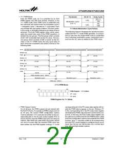
PA3 is pin-shared with the signal. If the PFD option is selected and if PA3 is setup as an output, then the output signal
on the PA3 pin will be the PFD signal, generated by the timer/event counter overflow signal. If setup as an input it will
function as a normal input pin. Once the PFD option is selected, the PFD output signal is controlled by the PA3 data reg-
ister only. Writing a ²1² to the PA3 data register will enable the PFD output function while writing a ²0² will force the PA3
pin to remain at ²0². The I/O functions of PA3 are shown below.
I/O Mode
I/P (Normal)
O/P (Normal)
I/P (PFD)
O/P (PFD)
PA3
Logical Input
Logical Output
Logical Input
PFD (Timer on)
Note: ThePFDfrequencyisthetimer/eventcounteroverflowfrequencydividedby2.
Rev. 1.20
23
October 2, 2007

 HOLTEK [ HOLTEK SEMICONDUCTOR INC ]