HT46R23/HT46C23
The A/D converter control register is used to control the
A/D converter. The bit2~bit0 of the ADCR are used to
select an analog input channel. There are a total of eight
channels to select. The bit5~bit3 of the ADCR are used
to set PB configurations. PB can be an analog input or
as digital I/O line decided by these 3 bits. Once a PB line
is selected as an analog input, the I/O functions and
pull-high resistor of this I/O line are disabled and the A/D
converter circuit is power on. The EOCB bit (bit6 of the
ADCR) is end of A/D conversion flag. Check this bit to
know when A/D conversion is completed. The START
bit of the ADCR is used to begin the conversion of the
A/D converter. Giving START bit a rising edge and fall-
ing edge means that the A/D conversion has started. In
order to ensure the A/D conversion is completed, the
START should remain at ²0² until the EOCB is cleared
to ²0² (end of A/D conversion).
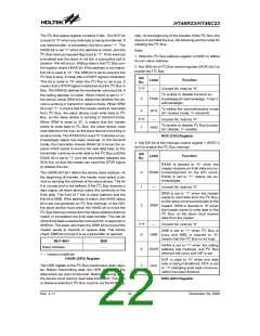
Bit No.
Label
Function
Selects the A/D converter
clock source
0
1
ADCS0 00= system clock/2
ADCS1 01= system clock/8
10= system clock/32
11= undefined
2~6
7
¾
Unused bit, read as ²0²
TEST
For test mode used only
ACSR (27H) Register
Bit No. Label
Function
0
1
2
ACS0
ACS1 Defines the analog channel select.
ACS2
3
4
5
PCR0
Defines the port B configuration select. If PCR0, PCR1 and PCR2 are all zero, the ADC circuit
is power off to reduce power consumption
PCR1
PCR2
Indicates end of A/D conversion. (0 = end of A/D conversion)
Each time bits 3~5 change state the A/D should be initialized by issuing a START signal, other-
wise the EOCB flag may have an undefined condition. See ²Important note for A/D initialization².
6
7
EOCB
START
Starts the A/D conversion. (0®1®0= start; 0®1= Reset A/D converter and set EOCB to ²1²)
ADCR (26H) Register
PCR2
PCR1
PCR0
7
6
5
4
3
2
1
0
0
0
0
0
1
1
1
1
0
0
1
1
0
0
1
1
0
1
0
1
0
1
0
1
PB7
PB7
PB7
PB7
PB7
PB7
PB7
AN7
PB6
PB6
PB6
PB6
PB6
PB6
PB6
AN6
PB5
PB5
PB5
PB5
PB5
PB5
AN5
AN5
PB4
PB4
PB4
PB4
PB4
AN4
AN4
AN4
PB3
PB3
PB3
PB3
AN3
AN3
AN3
AN3
PB2
PB2
PB2
AN2
AN2
AN2
AN2
AN2
PB1
PB1
AN1
AN1
AN1
AN1
AN1
AN1
PB0
AN0
AN0
AN0
AN0
AN0
AN0
AN0
Port B Configuration
ACS2
ACS1
ACS0
Analog Channel
0
0
0
0
1
1
1
1
0
0
1
1
0
0
1
1
0
AN0
AN1
AN2
AN3
AN4
AN5
AN6
AN7
1
0
1
0
1
0
1
Analog Input Channel Selection
Rev. 2.11
18
December 29, 2008
图片预览")
 HOLTEK [ HOLTEK SEMICONDUCTOR INC ]