HT46R23/HT46C23
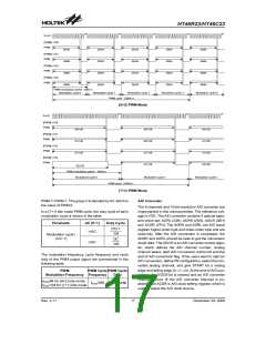
I2C Bus Serial Interface
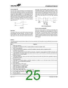
Low Voltage Reset - LVR
I2C Bus is implemented in the device. The I2C Bus is a
bidirectional two-wire lines. The data line and clock line
are implement in SDA pin and SCL pin. The SDA and
SCL are NMOS open drain output pin. They must con-
nect a pull-high resistor respectively.
The microcontroller provides low voltage reset circuit in
order to monitor the supply voltage of the device. If the
supply voltage of the device is within the range
0.9V~3.3V, such as changing a battery, the LVR will au-
tomatically reset the device internally.
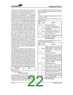
Using the I2C Bus, the device has two ways to transfer
data. One is in slave transmit mode, the other is in slave
receive mode. There are four registers related to I2C
Bus; HADR([20H]), HCR([21H]), HSR([22H]),
HDR([23H]). The HADR register is the slave address
setting of the device, if the master sends the calling ad-
dress which match, it means that this device is selected.
The HCR is I2C Bus control register which defines the
device enable or disable the I2C Bus as a transmitter or
as a receiver. The HSR is I2C Bus status register, it re-
sponds with the I2C Bus status. The HDR is input/output
data register, data to transmit or receive must be via the
HDR register.
The LVR includes the following specifications:
·
The low voltage (0.9V~VLVR) has to remain in their
original state to exceed 1ms. If the low voltage state
does not exceed 1ms, the LVR will ignore it and do not
perform a reset function.
·
The LVR uses the ²OR² function with the external RES
signal to perform chip reset.
The relationship between VDD and VLVR is shown below.
V
D
D
V
O P R
5
.
5
V
5
.
5
V
The I2C Bus control register contains three bits. The
HEN bit define the enable or disable the I2C Bus. If the
data wants transfer via I2C Bus, this bit must be set. The
HTX bit defines whether the I2C Bus is in transmit or re-
ceive mode. If the device is as a transmitter, this bit must
be set to ²1². The TXAK defines the transmit acknowl-
edge signal, when the device received 8-bit data, the
device sends this bit to I2C Bus at the 9th clock. If the re-
ceiver wants to continue to receive the next data, this bit
must be reset to ²0² before receiving data.
V
L
V
R
3
.
0
V
2
.
2
V
0
.
9
V
Note: VOPR is the voltage range for proper chip
operation at 4MHz system clock.
V
D
D
5
.
5
V
L
V
R
D
e
t
e
c
t
V
o
l
t
a
g
e
V
L
V
R
0
.
9
0
V
V
R
e
s
e
t
S
i
g
n
a
l
R
e
s
e
t
N
o
r
m
a
l
O
p
e
r
a
t
i
o
n
R
e
s
e
t
*
1
*
2
Low Voltage Reset
Note: *1: To make sure that the system oscillator has stabilized, the SST provides an extra delay of 1024 system
clock pulses before entering the normal operation.
*2: Since low voltage state has to be maintained in its original state for over 1ms, therefore after 1ms delay,
the device enters the reset mode.
Rev. 2.11
21
December 29, 2008
图片预览")
 HOLTEK [ HOLTEK SEMICONDUCTOR INC ]