HT46R23/HT46C23
S
Y
S
[
P
W
M
]
=
1
0
0
P
W
M
2
5
/
6
4
2
2
2
2
5
5
6
6
/
/
/
/
6
6
6
6
4
4
4
4
2
5
/
6
4
2
5
/
6
4
2
2
2
2
5
6
6
6
/
/
/
/
6
6
6
6
4
4
4
4
[
P
W
M
]
=
1
0
1
P
W
M
2
2
2
6
6
6
/
/
/
6
6
6
4
4
4
2
5
/
6
4
2
5
/
6
4
[
P
W
M
]
=
1
0
2
P
W
M
2
5
/
6
4
2
5
/
6
4
[
P
W
M
]
=
1
0
3
P
W
M
2
6
/
6
4
2
5
/
6
4
P
W
M
m
o
d
u
l
a
t
i
o
n
p
e
r
i
o
d
:
6
4
/
f
M
o
d
u
l
a
t
i
o
n
c
y
c
l
e
0
M
o
d
u
l
a
t
i
o
n
c
y
c
l
e
1
M
o
d
u
l
a
t
i
o
n
c
y
c
l
e
2
M
o
d
u
l
a
t
i
o
n
c
y
c
l
e
3
M
o
d
u
l
a
t
i
o
n
c
y
c
l
e
0
P
W
M
c
y
c
l
e
:
2
5
6
/
f
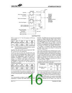
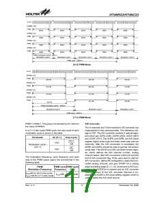
(6+2) PWM Mode
S
Y
S
[
P
W
M
]
=
1
0
0
P
W
M
5
5
5
0
1
1
/
/
/
1
1
1
2
2
2
8
8
8
5
0
/
1
2
8
5
0
/
1
2
8
[
P
W
M
]
=
1
0
1
P
W
M
5
0
/
1
2
8
5
1
/
1
2
8
[
P
W
M
]
=
1
0
2
P
W
M
5
1
/
1
2
8
5
1
/
1
2
8
[
P
W
M
]
=
1
0
3
P
W
M
5
1
/
1
2
8
5
2
/
1
2
8
5
2
/
1
2
8
P
W
M
m
o
d
u
l
a
t
i
o
n
p
e
r
i
o
d
:
1
2
8
/
f
M
o
d
u
l
a
t
i
o
n
c
y
c
l
e
0
M
o
d
u
l
a
t
i
o
n
c
y
c
l
e
1
M
o
d
u
l
a
t
i
o
n
c
y
c
l
e
0
P
W
M
c
y
c
l
e
:
2
5
6
/
f
(7+1) PWM Mode
PWM.7~PWM.1. The group 2 is denoted by AC which is
the value of PWM.0.
A/D Converter
The 8 channels and 10-bit resolution A/D converter are
implemented in this microcontroller. The reference volt-
age is VDD. The A/D converter contains 4 special regis-
ters which are; ADRL (24H), ADRH (25H), ADCR (26H)
and ACSR (27H). The ADRH and ADRL are A/D result
register higher-order byte and lower-order byte and are
read-only. After the A/D conversion is completed, the
ADRH and ADRL should be read to get the conversion
result data. The ADCR is an A/D converter control regis-
ter, which defines the A/D channel number, analog
channel select, start A/D conversion control bit and the
end of A/D conversion flag. If the users want to start an
A/D conversion, define PB configuration, select the con-
verted analog channel, and give START bit a raising
edge and falling edge (0®1®0). At the end of A/D con-
version, the EOCB bit is cleared and an A/D converter
interrupt occurs (if the A/D converter interrupt is en-
abled). The ACSR is A/D clock setting register, which is
used to select the A/D clock source.
In a (7+1) bits mode PWM cycle, the duty cycle of each
modulation cycle is shown in the table.
Parameter
AC (0~1)
Duty Cycle
DC+1
128
i<AC
Modulation cycle i
(i=0~1)
DC
i³AC
128
The modulation frequency, cycle frequency and cycle
duty of the PWM output signal are summarized in the
following table.
PWM
PWM Cycle PWM Cycle
Modulation Frequency Frequency
Duty
f
f
SYS/64 for (6+2) bits mode
f
SYS/256
[PWM]/256
SYS/128 for (7+1) bits mode
Rev. 2.11
17
December 29, 2008
图片预览")
 HOLTEK [ HOLTEK SEMICONDUCTOR INC ]