HT46R23/HT46C23
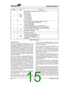
V
D
D
C
o
n
t
r
o
l
B
i
t
P
U
D
Q
D
a
t
a
B
u
s
P
A
0
~
P
A
2
W
r
i
t
e
C
o
n
t
r
o
l
R
e
g
i
s
t
e
r
C
K
Q
P
A
3
/
P
F
D
S
C
h
i
p
R
e
s
e
t
P
A
4
/
T
M
R
P
A
5
/
I
N
T
P
A
6
/
S
D
A
P
A
7
0
/
/
S
A
C
N
L
0
R
e
a
d
C
o
n
t
r
o
l
R
e
g
i
s
t
e
r
D
a
t
a
B
i
t
P
B
~
P
B
7
/
A
N
7
P
C
0
~
P
C
4
D
C
Q
P
P
D
D
0
1
/
/
P
W
M
0
P
W
M
1
K
Q
W
r
i
t
e
D
a
t
a
R
e
g
i
s
t
e
r
S
M
U
( P D 0 o r P W M 0 )
P
A
3
X
(
P
D
1
o
r
P
W
M
1
)
P
F
D
E
N
M
(
P
A
3
)
U
X
R
e
a
d
D
a
t
a
R
e
g
i
s
t
e
r
S
y
s
t
e
m
W
a
k
e
-
u
p
O
P
0
~
O
P
7
(
P
A
o
n
l
y
)
I
N
T
f
o
r
P
A
5
O
n
l
y
T
M
R
f
o
r
P
A
4
O
n
l
y
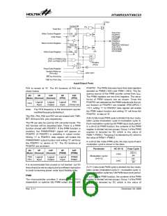
Input/Output Ports
PD0/PD1. The PWM channels have their data registers
denoted as PWM0 (1AH) and PWM1 (1BH). The fre-
PA3 to remain at ²0². The I/O functions of PA3 are
shown below.
quency source of the PWM counter comes from fSYS
.
I/O
I/P
O/P
I/P
O/P
The PWM registers are two 8-bit registers. The wave-
forms of PWM outputs are as shown. Once the
PD0/PD1 are selected as the PWM outputs and the out-
put function of PD0/PD1 are enabled (PDC.0/PDC.1
=²0²), writing ²1² to PD0/PD1 data register will enable
the PWM output function and writing ²0² will force the
PD0/PD1 to stay at ²0².
Mode (Normal) (Normal)
(PFD)
(PFD)
Logical
Input
Logical
Output
Logical
Input
PFD
PA3
(Timer on)
Note: The PFD frequency is the timer/event counter
overflowfrequencydividedby2.
The PA4, PA5, PA6 and PA7 are pin-shared with TMR,
INT, SDA and SCL pins respectively.
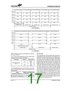
A (6+2) bits mode PWM cycle is divided into four modu-
lation cycles (modulation cycle 0~modulation cycle 3).
Each modulation cycle has 64 PWM input clock period.
In a (6+2) bit PWM function, the contents of the PWM
register is divided into two groups. Group 1 of the PWM
register is denoted by DC which is the value of
PWM.7~PWM.2. The group 2 is denoted by AC which is
the value of PWM.1~PWM.0.
The PB can also be used as A/D converter inputs. The
A/D function will be described later. There is a PWM
function shared with PD0/PD1. If the PWM function is
enabled, the PWM0/PWM1 signal will appear on
PD0/PD1 (if PD0/PD1 is operating in output mode).
Writing ²1² to PD0/PD1 data register will enable the
PWM0/PWM1 output function and writing ²0² will force
the PD0/PD1 to remain at ²0². The I/O functions of
PD0/PD1 are as shown.
In a (6+2) bits mode PWM cycle, the duty cycle of each
modulation cycle is shown in the table.
Parameter
AC (0~3)
Duty Cycle
I/O
I/P
O/P
I/P
O/P
DC+1
64
Mode (Normal) (Normal)
(PWM)
(PWM)
i<AC
Modulation cycle i
(i=0~3)
PD0
PD1
Logical
Input
Logical
Output
Logical
Input
PWM0
PWM1
DC
64
i³AC
It is recommended that unused or not bonded out I/O
lines should be set as output pins by software instruction
to avoid consuming power under input floating state.
A (7+1) bits mode PWM cycle is divided into two modu-
lation cycles (modulation cycle 0 ~ modulation cycle 1).
Each modulation cycle has 128 PWM input clock period.
PWM
In a (7+1) bits PWM function, the contents of the PWM
register is divided into two groups. Group 1 of the PWM
register is denoted by DC which is the value of
The microcontroller provides 2 channels (6+2)/(7+1)
(dependent on options) bits PWM output shared with
Rev. 2.11
16
December 29, 2008
图片预览")
 HOLTEK [ HOLTEK SEMICONDUCTOR INC ]