HT46R12
V
D
D
C
o
n
t
r
o
l
B
i
t
P
U
D
a
t
a
B
u
s
D
Q
P
A
0
~
P
A
2
W
r
i
t
e
C
o
n
t
r
o
l
R
e
g
i
s
t
e
r
C
K
Q
P
A
3
/
P
T
F
D
S
C
h
i
p
R
e
s
e
t
P
A
4
/
M
R
0
P
A
5
~
P
A
6
P
A
7
0
/
/
T
A
M
R
1
P
B
N
0
~
P
B
3
/
A
N
3
R
e
a
d
C
o
n
t
r
o
l
R
e
g
i
s
t
e
r
D
a
t
a
B
i
t
P
C
0
/
C
0
V
I
N
-
P
C
1
/
C
0
V
I
N
+
D
C
Q
P
P
C
C
2
3
/
/
C
C
0
1
O
O
U
T
U
T
K
Q
W
r
i
t
e
D
a
t
a
R
e
g
i
s
t
e
r
S
M
U
(
P
A
0
)
P
A
3
X
(
P
P
G
1
)
P
F
D
E
N
M
(
P
F
D
)
U
X
R
e
a
d
D
a
t
a
R
e
g
i
s
t
e
r
S
y
s
t
e
m
W
a
k
e
-
u
p
(
P
A
o
n
l
y
)
O
P
0
~
O
P
7
T
M
R
0
f
o
r
P
A
4
O
n
l
y
T
M
R
1
f
o
r
P
A
7
O
n
l
y
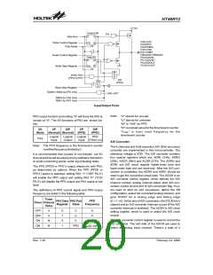
Input/Output Ports
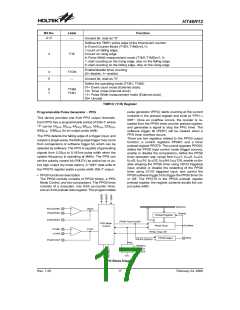
Note:
²X² stands for unused
PFD output function and writing ²0² will force the PA3 to
remain at ²0². The I/O functions of PA3 are shown be-
low.
²U² stands for unknown
²M² is ²256² for PFD
²N² is preload value for the timer/event counter
²fTMR² is input clock frequency for the
timer/event counter
I/O
I/P
O/P
I/P
O/P
Mode (Normal) (Normal) (PFD)
(PFD)
Logical
Input
Logical
Output
Logical
PFD
PA3
Input (Timer on)
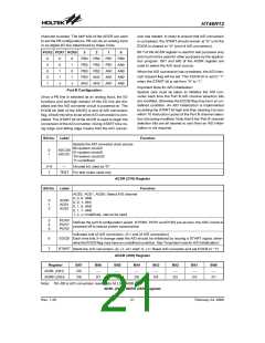
A/D Converter
Note: The PFD frequency is the timer/event counter
overflowfrequencydividedby2.
The 4 channels and 9-bit resolution A/D (8-bit accuracy)
converter are implemented in this microcontroller. The
reference voltage is VDD. The A/D converter contains
four special registers which are; ADRL (24H), ADRH
(25H), ADCR (26H) and ACSR (27H). The ADRH and
ADRL are A/D result register higher-order byte and
lower-order byte and are read-only. After the A/D con-
version is completed, the ADRH and ADRL should be
read to get the conversion result data. The ADCR is an
A/D converter control register, which defines the A/D
channel number, analog channel select, start A/D con-
version control bit and end of A/D conversion flag. If us-
ers want to start an A/D conversion, define the PB
configuration, select the converted analog channel, and
give START bit a raising edge and falling edge
(0®1®0). At the end of A/D conversion, the EOCB bit is
cleared and an A/D converter interrupt occurs (if the A/D
converter interrupt is enabled). The ACSR is A/D clock
setting register, which is used to select the A/D clock
source.
It is recommended that unused or not bonded out I/O
lines should be set as output pins by software instruction
to avoid consuming power under input floating state.
The PFD (PFD0 or PFD1) output shares pin with PA3,
as determined by options. When the PFD (PFD0 or
PFD1) option is selected, setting PA3 ²1² (²SET PA.3²)
will enable the PFD output and setting PA3 ²0² (²CLR
PA.3²) will disable the PFD output and PA3 output at low
level.
The definitions of PFD control signal and PFD output
frequency are listed in the following table.
Timer
PA3 Data PA3 Pad
PFD
Timer Preload
Value
Register
State
Frequency
OFF
OFF
ON
X
X
N
N
0
1
0
1
0
U
X
X
The A/D converter control register is used to control the
A/D converter. The bit2~bit0 of the ADCR are used to
select an analog input channel. There¢s a total of 4
0
X
ON
PFD
f
TMR/[2´(M-N)]
Rev. 1.20
20
February 24, 2006
图片预览")
 HOLTEK [ HOLTEK SEMICONDUCTOR INC ]