HT46R12
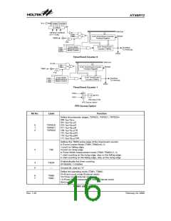
The P0SPEN is the PPG0 timer OFF enable or disable bit using C0VO trigger input, if this bit is enabled, the PPG0
stopping input can be triggered by C0VO or PC2 falling edge. The P0RSEN is the PPG0 restarting enable or disable
bit using C1VO trigger input, if this bit is enabled, the PPG0 timer restarting input can be trigger by C1VO or PC3 fall-
ing edge. User can read the status of C0VO or C1VO by setting the PC2 or PC3 to be an input pin when comparator 0
or comparator 1 is enabled.
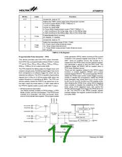
P0SPEN
Description
Disable stopping the PPG0 timer using C0VO trigger input.
0
PPG0 module output can be stopped by software control (P0ST) only.
Enable stopping the PPG0 timer using C0VO trigger input.
PPG0 module output can be stopped by C0VO falling edge trigger or software control (P0ST bit is
cleared to ²0²).
1
P0RSEN
Description
Disable restarting the PPG0 timer using C1VO trigger input.
0
PPG0 module output can be restarted by software control (P0ST) only.
Enable restarting the PPG0 timer using C1VO trigger input.
PPG0 module output can be restarted by C1VO falling edge trigger or software control (P0ST is set to
1
²1²)
The P0ST is a software trigger bit, if this bit is set to ²1², the PPG0 timer will start counting and this bit will be cleared
when the PPG timer overflow occurs, if this bit is cleared to ²0², the PPG0 timer will stop counting, when the PPG
timer is counting and if a falling edge generates from C1VO, PC3 or a software control bit (P0ST) is set, the PPG0
timer counter is not affected, the trigger from C1V0, PC3 or P0ST is not useful. The P0ST can also be used as a sta-
tus bit of PPG0 timer output.
Input/Output Ports
Each bit of these input/output latches can be set or
cleared by ²SET [m].i² and ²CLR [m].i² (m=12H, 14H or
16H) instructions.
There are 16 bidirectional input/output lines in the
microcontroller, labeled as PA, PB and PC, which are
mapped to the data memory of [12H], [14H] and [16H]
respectively. All of these I/O ports can be used for input
and output operations. For input operation, these ports
are non-latching, that is, the inputs must be ready at the
T2 rising edge of instruction ²MOV A,[m]² (m=12H, 14H
or 16H). For output operation, all the data is latched and
remains unchanged until the output latch is rewritten.
Some instructions first input data and then follow the
output operations. For example, ²SET [m].i², ²CLR
[m].i², ²CPL [m]², ²CPLA [m]² read the entire port states
into the CPU, execute the defined operations
(bit-operation), and then write the results back to the
latches or the accumulator.
Each line of port A has the capability of waking-up the
device.
Each I/O line has its own control register (PAC, PBC,
PCC) to control the input/output configuration. With this
control register, CMOS output or Schmitt trigger input
with or without pull-high resistor structures can be re-
configured dynamically under software control. To func-
tion as an input, the corresponding latch of the control
register must write ²1². The input source also depends
on the control register. If the control register bit is ²1²,
the input will read the pad state. If the control register bit
is ²0², the contents of the latches will move to the inter-
nal bus. The latter is possible in the ²read-modify-write²
instruction.
Each I/O port has a pull-high option. Once the pull-high
option is selected, the I/O port has a pull-high resistor,
otherwise, there¢s none. Take note that a non-pull-high
I/O port operating in input mode will cause a floating
state.
The PA3, PA4 and PA7 are pin-shared with PFD, TMR0
and TMR1 pins respectively. And the PC0, PC1, PC2
and PC3 are pin-shared with C0VIN1-, C0VIN+,
C0OUT, C1OUT.
The PA3 is pin-shared with the PFD signal. If the PFD
option is selected, the output signal in output mode of
PA3 will be the PFD signal generated by a timer/event
counter overflow signal. The input mode always remain
in its original functions. Once the PFD option is selected,
the PFD output signal is controlled by the PA3 data reg-
ister only. Writing ²1² to PA3 data register will enable the
For output function, CMOS is the only configuration.
These control registers are mapped to locations 13H,
15H and 17H.
After a chip reset, these input/output lines remain at high
levels or floating state (depending on pull-high options).
Rev. 1.20
19
February 24, 2006
图片预览")
 HOLTEK [ HOLTEK SEMICONDUCTOR INC ]