HT46R12
Bit No.
Label
Function
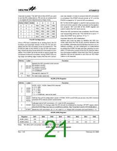
0~2
¾
Unused bit, read as ²0²
Defines the TMR1 active edge of the timer/event counter:
In Event Counter Mode (T1M1,T1M0)=(0,1):
1:count on falling edge;
3
T1E
0:count on rising edge
In Pulse Width measurement mode (T1M1,T1M0)=(1,1):
1: start counting on the rising edge, stop on the falling edge;
0: start counting on the falling edge, stop on the rising edge
Enable/disable timer counting
(0= disable; 1= enable)
4
5
T1ON
¾
Unused bit, read as ²0²
Define the operating mode (T1M1, T1M0)
01= Event count mode (External clock)
10= Timer mode (Internal clock)
6
7
T1M0
T1M1
11= Pulse Width measurement mode (External clock)
00= Unused
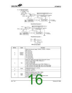
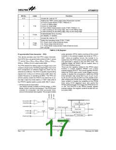
TMR1C (11H) Register
pulse generator (PPG) starts counting at the current
contents in the preload register and ends at ²FFH®
00H². Once an overflow occurs, the counter is re-
loaded from the PPG0 timer counter preload register,
and generates a signal to stop the PPG timer. The
software trigger bit (P0ST) will be cleared when a
PPG timer overflow occurs.
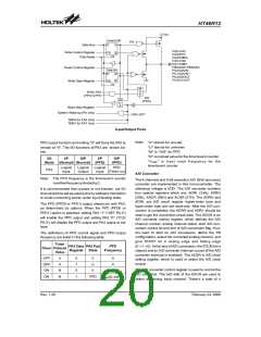
Programmable Pulse Generator - PPG
This device provides one 8-bit PPG output channels.
Each PPG has a programmable period of 256´T, where
²T² can be 1/fSYS, 2/fSYS, 4/fSYS, 8/fSYS, 16/fSYS, 32/fSYS
64/fSYS, 128/fSYS for an output pulse width.
,
The PPG detects the falling edge of a trigger input, and
outputs a single pulse, the falling edge trigger may come
from comparators or software trigger bit, which can be
selected by software. The PPG is capable of generating
signals from 0.25ms to 8.192ms pulse width when the
system frequency is operating at 4MHz. The PPG can
set the polarity control bit (P0LEV) as active low or ac-
tive high output (by mask option). A ²00H² data write to
the PPGT0 register yields a pulse width 256´T output.
There are two registers related to the PPG0 output
function, a control registers PPG0C and a timer
preload register PPGT0. The control registers PPG0C
define the PPG0 input control mode (trigger source),
enable or disable the comparators, define the PPG0
timer prescaler rate, range form fSYS/1, fSYS/2, fSYS/4,
fSYS/8, fSYS/16, fSYS/32, fSYS/64, fSYS/128, enable or dis-
able stopping the PPG0 timer using C0VO triggered
input, enable or disable the restarting of the PPG0
timer using C1VO triggered input, and control the
PPG0 software trigger bit to trigger the PPG0 timer On
or Off. The PPGT0 is the PPG0 preload register
preload register, the register contents decide the out-
put pulse width.
·
PPG0 functional description
The PPG0 module consists of PPG0 timers, a PPG
Mode Control, and two comparators. The PPG0 timer
consists of a prescaler, one 8-bit up-counter timer,
and an 8-bit preload data register. The programmable
D
a
t
a
b
u
s
P
C
1
/
C
0
V
I
N
+
+
C
0
V
O
P
C
0
/
C
0
V
I
N
-
-
R
e
l
o
a
d
P
r
e
l
o
a
d
R
e
g
i
s
t
e
r
P
C
2
/
C
0
O
U
T
P
P
G
0
T
i
m
e
r
O
n
/
O
f
f
P
P
G
M
o
d
e
O
v
e
r
f
l
o
w
P
P
G
0
T
i
m
e
r
C
o
n
t
r
o
l
C
1
V
I
N
+
+
C
1
V
O
P
P
G
0
T
i
m
e
r
O
f
f
C
1
V
I
N
-
-
P
P
G
0
O
u
t
p
u
t
P
P
G
P
0
L
E
V
(
O
p
t
i
o
n
)
P
C
3
/
C
1
O
U
T
P
0
f
s
P
0
P
S
C
2
P
r
e
s
c
a
l
e
r
P
0
P
S
C
1
P
0
P
S
C
0
f
S Y S
PPG Block Diagram
Rev. 1.20
17
February 24, 2006
图片预览")
 HOLTEK [ HOLTEK SEMICONDUCTOR INC ]