HT46R12
channels to select. The bit5~bit3 of the ADCR are used
to set the PB configurations. PB can be an analog input
or as digital I/O line determined by these 3 bits.
sion has started. In order to ensure that A/D conversion
is completed, the START should remain at ²0² until the
EOCB is cleared to ²0² (end of A/D conversion).
Bit 7 of the ACSR register is used for test purposes only
and must not be used for other purposes by the applica-
tion program. Bit1 and bit0 of the ACSR register are
used to select the A/D clock source.
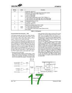
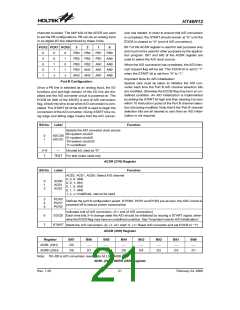
PCR2 PCR1 PCR0
3
2
1
0
0
0
0
0
1
0
0
1
1
x
0
1
0
1
x
PB3
PB3
PB3
PB3
PB2
PB2
PB2
PB1
PB1
PB0
AN0
AN1 AN0
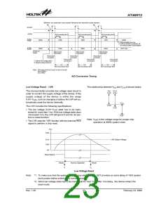
When the A/D conversion has completed, the A/D inter-
rupt request flag will be set. The EOCB bit is set to ²1²
when the START bit is set from ²0² to ²1².
AN2 AN1 AN0
AN3 AN2 AN1 AN0
Important Note for A/D initialization:
Port B Configuration
Special care must be taken to initialize the A/D con-
verter each time the Port B A/D channel selection bits
are modified, otherwise the EOCB flag may be in an un-
defined condition. An A/D initialization is implemented
by setting the START bit high and then clearing it to zero
within 10 instruction cycles of the Port B channel selec-
tion bits being modified. Note that if the Port B channel
selection bits are all cleared to zero then an A/D initial-
ization is not required.
Once a PB line is selected as an analog input, the I/O
functions and pull-high resistor of this I/O line are dis-
abled and the A/D converter circuit is powered on. The
EOCB bit (bit6 of the ADCR) is end of A/D conversion
flag. Check this bit to know when A/D conversion is com-
pleted. The START bit of the ADCR is used to begin the
conversion of the A/D converter. Giving START bit a ris-
ing edge and falling edge means that the A/D conver-
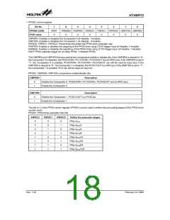
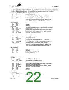
Bit No. Label
Function
Selects the A/D converter clock source
00=system clock/2
0
1
ADCS0
ADCS1
01=system clock/8
10=system clock/32
11=undefined
2~6
7
¾
Unused bit, read as ²0²
TEST For test mode used only
ACSR (27H) Register
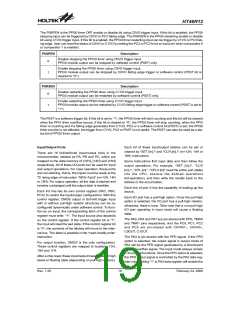
Bit No. Label
Function
ACS2, ACS1, ACS0: Select A/D channel
0, 0, 0: AN0
0
1
2
ACS0
ACS1
ACS2
0, 0, 1: AN1
0, 1, 0: AN2
0, 1, 1: AN3
1, x, x: Undefined, cannot be used
3
4
5
PCR0
PCR1
PCR2
Defines the port B configuration select. If PCR0, PCR1 and PCR2 are all zero, the ADC circuit is
powered off to reduce power consumption
Indicates end of A/D conversion. (0 = end of A/D conversion)
Each time bits 3~5 change state the A/D should be initialized by issuing a START signal, other-
wise the EOCB flag may have an undefined condition. See ²Important note for A/D initialization².
6
7
EOCB
START
Starts the A/D conversion. (0®1®0= start; 0®1= Reset A/D converter and set EOCB to ²1²)
ADCR (26H) Register
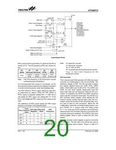
Register
ADRL (24H)
ADRH (25H)
Bit7
D0
Bit6
¾
Bit5
¾
Bit4
¾
Bit3
¾
Bit2
¾
Bit1
¾
Bit0
¾
D8
D7
D6
D5
D4
D3
D2
D1
Note: D0~D8 is A/D conversion result data bit LSB~MSB.
ADRL (24H), ADRH (25H) Register
Rev. 1.20
21
February 24, 2006
图片预览")
 HOLTEK [ HOLTEK SEMICONDUCTOR INC ]