Preliminary
HT45R04/HT45R04E
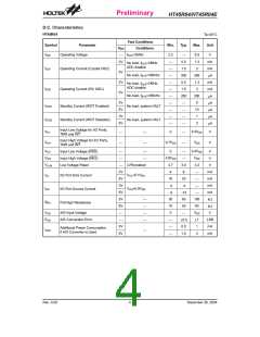
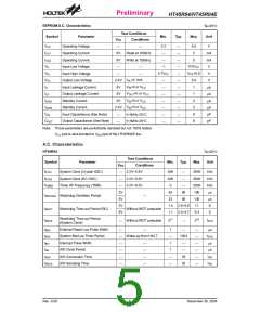
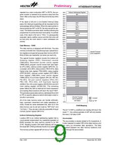
EEPROM D.C. Characteristics
Ta=25°C
Test Conditions
Symbol
Parameter
Operating Voltage
Min.
Typ.
Max.
Unit
VCC
¾
Conditions
¾
VCC
ICC1
ICC2
VIL
2.2
5.5
V
mA
mA
V
¾
¾
¾
¾
¾
¾
¾
¾
¾
¾
¾
¾
Operating Current
5V
5V
¾
Read at 100kHz
Write at 100kHz
2
5
¾
¾
Operating Current
0.3VCC
Input Low Voltage
¾
¾
-1
VIH
0.7VCC
V
CC+0.5
Input High Voltage
V
¾
VOL
ILI
IOL=2.1mA
VIN=0 or VCC
VOUT=0 or VCC
VIN=0 or VCC
VIN=0 or VCC
Output Low Voltage
Input Leakage Current
Output Leakage Current
Standby Current
2.4V
5V
5V
5V
2.4V
¾
0.4
1
V
¾
¾
¾
¾
¾
¾
¾
mA
mA
mA
mA
pF
pF
ILO
1
ISTB1
ISTB2
CIN
4
Standby Current
3
Input Capacitance (See Note)
Output Capacitance (See Note)
6
f=1MHz 25°C
f=1MHz 25°C
COUT
8
¾
Note: These parameters are periodically sampled but not 100% tested
VCC pad is wire-bonded to VDD pad of the HT45R04E die.
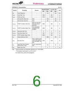
A.C. Characteristics
HT45R04
Ta=25°C
Test Conditions
Symbol
Parameter
Min.
Typ.
Max.
Unit
VDD
¾
Conditions
2.2V~5.5V
fSYS1
fSYS2
fTIMER
System Clock (Crystal OSC)
System Clock (RC OSC)
Timer I/P Frequency (TMR)
400
400
0
2000
2000
2000
180
kHz
kHz
kHz
¾
¾
¾
90
65
2.2V~5.5V
2.2V~5.5V
¾
¾
3V
5V
3V
5V
45
ms
ms
S
tWDTOSC
Watchdog Oscillator Period
¾
32
130
1.4 2.8~5.6
11
tWDT1
Watchdog Time-out Period (RC)
Without WDT prescaler
Without WDT prescaler
1.1 2.3~4.7 9.4
S
Watchdog Time-out Period
(System Clock)
217
218
tWDT2
tSYS
¾
¾
tRES
tSST
tINT
External Reset Low Pulse Width
System Start-up Timer Period
Interrupt Pulse Width
1
¾
1
¾
¾
¾
¾
¾
¾
¾
¾
1024
¾
¾
¾
¾
¾
¾
¾
ms
tSYS
Wake-up from HALT
¾
¾
¾
¾
ms
ms
tAD
A/D Clock Period
1
¾
tADC
tADCS
tAD
tAD
A/D Conversion Time
A/D Sampling Time
76
¾
¾
32
Rev. 0.00
5
December 30, 2004

 HOLTEK [ HOLTEK SEMICONDUCTOR INC ]