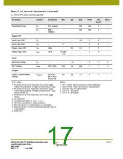
Table 1-1: Pin Descriptions (Continued)
Pin
Name
Timing
Type
Description
Number
G8
FIFO_LD
Synchronous
with PCLK
Output
CONTROL SIGNAL OUTPUT
Signal levels are LVCMOS/LVTTL compatible.
Used as a control signal for external FIFO(s).
Normally HIGH but will go LOW for one PCLK period at SAV.
H2
H4
TERM2
Analog
Input
Input
Termination for serial digital input 2. AC couple to EQ_GND.
CS_TMS
Synchronous
with
CONTROL SIGNAL INPUT
Signal levels are LVCMOS/LVTTL compatible.
SCLK_TCK
Chip Select/Test Mode Select
Host mode (JTAG/HOST = LOW)
CS_TMS operates as the Host Interface Chip Select, CS, and is active
LOW.
JTAG Test mode (JTAG/HOST = HIGH)
CS_TMS operates as the JTAG Test Mode Select, TMS, and is active
HIGH.
NOTE: If the Host Interface is not being used, tie this pin HIGH.
H5
SCLK_TCK
Non
Input
CONTROL SIGNAL INPUT
Synchronous
Signal levels are LVCMOS/LVTTL compatible.
Serial Data Clock/Test Clock.
Host mode (JTAG/HOST = LOW)
SCLK_TCK operates as the Host Interface Burst Clock, SCLK. Command
and data read/write words are clocked into the device synchronously
with this clock.
JTAG Test Mode (JTAG/HOST = HIGH)
SCLK_TCK operates as the JTAG test clock, TCK.
NOTE: If the Host Interface is not being used, tie this pin HIGH.
H6
SDOUT_TDO
Synchronous
with
Output
CONTROL SIGNAL OUTPUT
Signal levels are LVCMOS/LVTTL compatible.
SCLK_TCK
Serial Data Output/Test Data Output
Host mode (JTAG/HOST = LOW)
SDOUT_TDO operates as the Host Interface Serial Digital Output,
SDOUT, used to read status and configuration information from the
internal registers of the device.
JTAG Test Mode (JTAG/HOST = HIGH)
SDOUT_TDO operates as the JTAG test data output, TDO.
H7
DATA_ERROR
Synchronous
with PCLK
Output
STATUS SIGNAL OUTPUT
Signal levels are LVCMOS/LVTTL compatible.
The DATA_ERROR signal will be LOW when an error within the
received data stream has been detected by the device. This pin is a
logical 'OR'ing of all detectable errors listed in the internal
ERROR_STATUS register.
Once an error is detected, DATA_ERROR will remain LOW until the
start of the next video frame/field, or until the ERROR_STATUS register
is read via the Host Interface.
The DATA_ERROR signal will be HIGH when the received data stream
has been detected without error.
NOTE: It is possible to program which error conditions are monitored
by the device by setting appropriate bits of the ERROR_MASK register
HIGH. All error conditions are detected by default.
GS1559 HD-LINX™ II Multi-Rate Deserializer with
Loop-Through Cable Driver
Data Sheet
13 of 71
30572 - 8
July 2008

 GENNUM [ GENNUM CORPORATION ]