Table 1-1: Pin Descriptions (Continued)
Pin
Name
Timing
Type
Description
Number
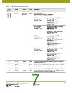
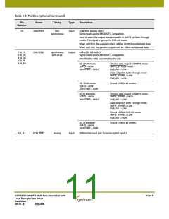
F4
20bit/10bit
Non
Input
CONTROL SIGNAL INPUT
Synchronous
Signal levels are LVCMOS/LVTTL compatible.
Used to select the output data bus width in SMPTE or Data-Through
modes. This signal is ignored in DVB-ASI mode.
When set HIGH, the parallel output will be 20-bit demultiplexed data.
When set LOW, the parallel outputs will be 10-bit multiplexed data.
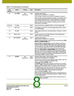
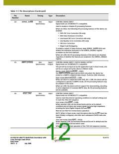
F10, F9,
G10, G9,
H10, H9,
J10, J9,
DOUT[9:0]
Synchronous
with PCLK
Output
PARALLEL DATA BUS
Signal levels are LVCMOS/LVTTL compatible.
DOUT9 is the MSB and DOUT0 is the LSB.
K10, K9
HD 20-bit mode
SD/HD = LOW
Chroma data output in SMPTE mode
SMPTE_BYPASS =HIGH
20bit/10bit = HIGH
DVB_ASI = LOW
Data output in Data-Through mode
SMPTE_BYPASS = LOW
DVB_ASI = LOW
HD 10-bit mode
SD/HD = LOW
Forced LOW in all modes.
20bit/10bit = LOW
SD 20-bit mode
SD/HD = HIGH
Chroma data output in SMPTE mode
SMPTE_BYPASS = HIGH
20bit/10bit = HIGH
DVB_ASI = LOW
Data output in Data-Through mode
SMPTE_BYPASS = LOW
DVB_ASI = LOW
Forced LOW in DVB-ASI mode
SMPTE_BYPASS = LOW
DVB_ASI = HIGH
SD 10-bit mode
SD/HD = HIGH
Forced LOW in all modes.
20bit/10bit = LOW
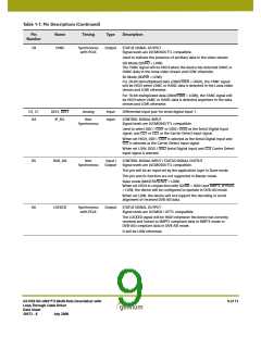
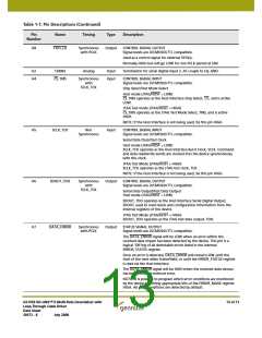
G1, H1
DDI2, DDI2
Analog
Input
Differential input pair for serial digital input 2.
GS1559 HD-LINX™ II Multi-Rate Deserializer with
Loop-Through Cable Driver
Data Sheet
11 of 71
30572 - 8
July 2008

 GENNUM [ GENNUM CORPORATION ]