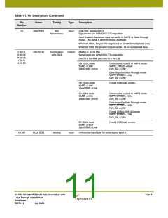
Table 1-1: Pin Descriptions (Continued)
Pin
Name
Timing
Type
Description
Number
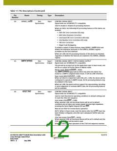
K1
RSET
Analog
Input
Used to set the serial digital loop-through output signal amplitude.
Connect to CD_VDD through 281Ω +/- 1% for 800mVp-p single-ended
output swing.
K2
CD_VDD
–
Power
Power Supply connection for the serial digital Cable Driver. Connect to
+1.8V DC analog.
K3, K4
SDO, SDO
Analog
Output
Serial digital loop-through output signal operating at 1.485Gb/s,
1.485/1.001Gb/s, or 270Mb/s.
The slew rate of these outputs is automatically controlled to meet
SMPTE 292M and 259M requirements according to the setting of the
SD/HD pin.
K5
K6
CD_GND
–
Power
Input
Ground connection for the serial digital Cable Driver. Connect to
analog GND.
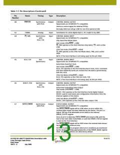
JTAG/HOST
Non
CONTROL SIGNAL INPUT
Synchronous
Signal levels are LVCMOS/LVTTL compatible.
Used to select JTAG Test mode or Host Interface mode.
When set HIGH, CS_TMS, SDOUT_TDO, SDI_TDI and SCLK_TCK are
configured for JTAG boundary scan testing.
When set LOW, CS_TMS, SDOUT_TDO, SDI_TDI and SCLK_TCK are
configured as GSPI pins for normal Host Interface operation.
K7
F
Synchronous
with PCLK
Output
STATUS SIGNAL OUTPUT
Signal levels are LVCMOS/LVTTL compatible.
Used to indicate the ODD/EVEN field of the video signal.
The F signal will be HIGH for the entire period of field 2 as indicated by
the F bit in the received TRS signals.
The F signal will be LOW for all lines in field 1 and for all lines in
progressive scan systems.
GS1559 HD-LINX™ II Multi-Rate Deserializer with
Loop-Through Cable Driver
Data Sheet
15 of 71
30572 - 8
July 2008

 GENNUM [ GENNUM CORPORATION ]