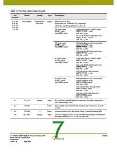
Table 1-1: Pin Descriptions (Continued)
Pin
Name
Timing
Type
Description
Number
B7
FW_EN/DIS
Non
Input
CONTROL SIGNAL INPUT
Synchronous
Signal levels are LVCMOS/LVTTL compatible.
Used to enable or disable the noise immune Flywheel of the device.
When set HIGH, the internal Flywheel is enabled. This Flywheel is used
in the extraction and generation of TRS timing signals, in automatic
video standards detection, and in manual switch line lock handling.
When set LOW, the internal Flywheel is disabled and TRS correction
and insertion is unavailable.
B8, F8, J8
C1
IO_GND
–
–
Power
Power
Ground connection for digital I/O buffers. Connect to digital GND.
BUFF_VDD
Power Supply connection for the Serial Digital Input buffers. Connect
to +1.8V DC analog.
C2
C3
C6
PD_VDD
–
–
Power
Power
Input
Power Supply connection for the Phase Detector. Connect to +1.8V DC
analog.
PDBUFF_GND
MASTER/SLAVE
Ground connection for the Phase Detector and Serial Digital Input
buffers. Connect to analog GND.
Non
CONTROL SIGNAL INPUT
Synchronous
Signal levels are LVCMOS/LVTTL compatible.
Used to determine the input / output selection for the DVB_ASI, SD/HD,
RC_BYP and SMPTE_BYPASS pins.
When set HIGH, the GS1559 is set to operate in Master mode where
SD/HD, RC_BYP and SMPTE_BYPASS become status signal output pins
set by the device. In this mode, the GS1559 will automatically detect,
reclock, deserialize and process SD SMPTE and HD SMPTE input data.
When set LOW, the GS1559 is set to operate in Slave mode where
DVB_ASI, SD/HD, RC_BYP and SMPTE_BYPASS become control signal
input pins. In this mode, the application layer must set these external
device pins for the correct reception of either SMPTE or DVB-ASI data.
Slave mode also supports the reclocking and deserializing of data not
conforming to SMPTE or DVB-ASI streams.
C7
RC_BYP
Non
Synchronous
Input
/Output
CONTROL SIGNAL INPUT / STATUS SIGNAL OUTPUT
Signal levels are LVCMOS/LVTTL compatible.
This pin will be an input set by the application layer in Slave mode, and
will be an output set by the device in Master mode.
Master mode (MASTER/SLAVE = HIGH)
The RC_BYP signal will be HIGH only when the device has successfully
locked to a SMPTE compliant input data stream. In this case, the serial
digital loop-through output will be a reclocked version of the input.
The RC_BYP signal will be LOW whenever the input does not conform
to a SMPTE compliant data stream. In this case, the serial digital
loop-through output will be a buffered version of the input.
Slave mode (MASTER/SLAVE = LOW)
When set HIGH, the serial digital output will be a reclocked version of
the input signal regardless of whether the device is in SMPTE, DVB-ASI
or Data-Through mode.
When set LOW, the serial digital output will be a buffered version of
the input signal in all modes.
GS1559 HD-LINX™ II Multi-Rate Deserializer with
Loop-Through Cable Driver
Data Sheet
8 of 71
30572 - 8
July 2008

 GENNUM [ GENNUM CORPORATION ]