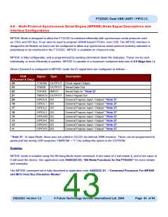
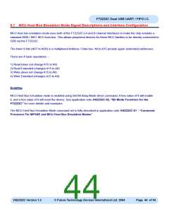
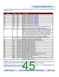
FT2232C Dual USB UART / FIFO I.C.
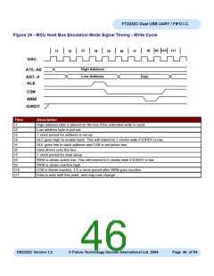
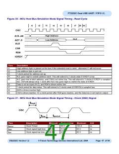
Figure 30 - MCU Host Bus Emulation Mode Signal Timing - Read Cycle
t3
t1
t2
t4
t5
t6
t7
t8 t9
OSC
High Address
Low Address
A15..A8
Hi-Z
AD7..0
ALE
CS#
RD#
IORDY
Time
t1
Description
High address byte is placed on the bus if the extended read is used - otherwise t1 will not occur.
Low address byte is put out.
t2
t3
1 clock period for address set up.
t4
ALE goes high to enable address latch. This will extend to 2 clocks wide if IORDY is low.
t5
ALE goes low to latch address, and CS# is set active low. This will extend to 3 clocks if IORDY is sampled
low. CS# will always drop 1 clock after ALE has gone high no matter the state of IORDY.
t6
t7
t8
t9
Data is set as input (Hi-Z), and RD# is driven active low.
1 clock period for data setup. This will extend to 5 clocks wide if IORDY# is sampled low.
RD# is driven inactive high.
CS# is driven inactive 1/2 a clock period after RD# goes inactive, and the data bus is set back to output.
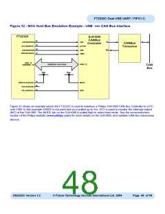
Figure 31 - MCU Host Bus Emulation Mode Signal Timing - Clock (OSC) Signal
t
high
OSC
t
period
t
low
Time
tperiod
thigh
Description
Minimum
41.6
Typical Value
83.3
Maximum
125.0
62.5
Unit
ns
Clock Period
Clock signal high time
Clock signal low time
20.8
41.6
ns
20.8
41.6
62.5
ns
tlow
DS2232C Version 1.2
© Future Technology Devices International Ltd. 2004
Page 47 of 54

 FTDI [ FUTURE TECHNOLOGY DEVICES INTERNATIONAL LTD. ]