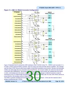
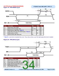
245 FIFO Mode TIMING DIAGRAMS
Figure 19 - FIFO READ Cycle
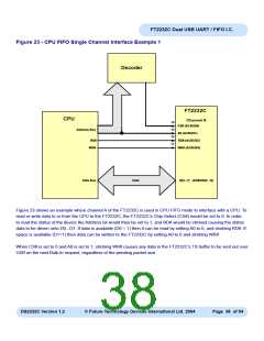
FT2232C Dual USB UART / FIFO I.C.
T6
T5
RXF#
RD#
T2
T1
T4
T3
Valid Data
D[7...0]
Time
T1
Description
Min
Max
Unit
ns
ns
ns
ns
ns
ns
RD# Active Pulse Width
RD# to RD Pre-Charge Time
RD# Active to Valid Data **Note 19
50
T2
50 + T6
T3
20
0
50
25
T4
Valid Data Hold Time from RD# Inactive **Note 19
RD# Inactive to RXF#
T5
0
T6
RXF# inactive after RD# cycle
80
** Note 19 : Load 30 pF at standard drive level. These times will also vary if the high output drive level is enabled.
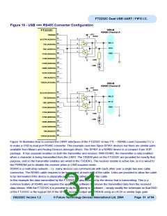
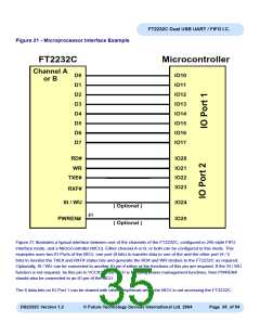
Figure 20 - FIFO Write Cycle
T12
T11
TXE#
T8
T7
WR
T9
T10
Valid Data
D[7...0]
Time
T7
Description
Min
50
50
20
0
Max
Unit
ns
ns
ns
ns
ns
ns
WR Active Pulse Width
T8
WR to WR Pre-Charge Time
Data Setup Time before WR inactive
Data Hold Time from WR inactive
WR Inactive to TXE#
T9
T10
T11
T12
5
25
TXE inactive after WR cycle
80
DS2232C Version 1.2
© Future Technology Devices International Ltd. 2004
Page 34 of 54

 FTDI [ FUTURE TECHNOLOGY DEVICES INTERNATIONAL LTD. ]