FT2232C Dual USB UART / FIFO I.C.
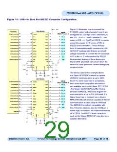
Figure 15 - USB <=> RS422 Converter Configuration
VCC
14 SP491
FT2232C
DB9-M
RS422 Channel A
41
13
4
PWREN#
10
9
TXDM_A
5
3
2
SLEEP# (ACBUS1)
D
TXDP_A
RXDP_A
24
23
22
21
20
19
17
16
15
TXD (ADBUS0)
RXD (ADBUS1)
RTS# (ADBUS2)
CTS# (ADBUS3)
DTR# (ADBUS4)
DSR# (ADBUS5)
DCD# (ADBUS6)
RI# (ADBUS7)
11
12
120R
R
RXDM_A
6
7
VCC
14 SP491
GND
4
10
9
RTSM_A
5
3
2
D
RTSP_A
CTSP_A
11
120R
R
12
CTSM_A
6
7
TXDEN (ACBUS0)
VCC
14 SP491
DB9-M
RS422 Channel B
4
29
40
39
38
37
36
35
33
32
30
SLEEP# (BCBUS1)
TXD (BDBUS0)
RXD (BDBUS1)
RTS# (BDBUS2)
CTS# (BDBUS3)
DTR# (BDBUS4)
DSR# (BDBUS5)
DCD# (BDBUS6)
RI# (BDBUS7)
10
9
TXDM_B
5
3
2
D
TXDP_B
RXDP_B
11
120R
R
12
RXDM_B
6
7
VCC
14 SP491
GND
4
10
9
RTSM_B
5
3
2
D
RTSP_B
CTSP_B
11
120R
R
12
TXDEN (BCBUS0)
CTSM_B
6
7
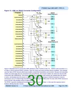
Figure 15 illustrates how to connect the UART interfaces of the FT2232C to two TTL – RS422 Level Converter I.C.’s
to make a USB to dual port RS422 converter. There are many such level converter devices available – this example
uses two Sipex SP491 devices which have enables on both their transmitters and receivers. Because the transmitter
enables are active high, they are connected to the SLEEP# pins. The receiver enables are active low and are both
connected to the PWREN# pin. This ensures that both the transmitters and receivers are enabled when the device
is active, and disabled when the device is in USB suspend mode. If the design is USB BUS powered, it may be
necessary to use a P-Channel logic level MOSFET (controlled by PWREN#) in the VCC line of the SP491 devices to
ensure that the USB standby current of 500μA is met.
The SP491 is good for sending and receiving data at a rate of up to 5M Baud – in this case the maximum rate is
limited to 3M Baud by the FT2232C.
DS2232C Version 1.2
© Future Technology Devices International Ltd. 2004
Page 30 of 54

 FTDI [ FUTURE TECHNOLOGY DEVICES INTERNATIONAL LTD. ]