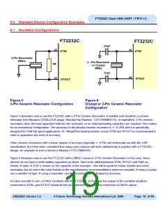
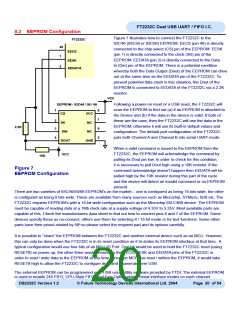
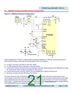
FT2232C Dual USB UART / FIFO I.C.
8.4 Interfacing to 3.3V Logic
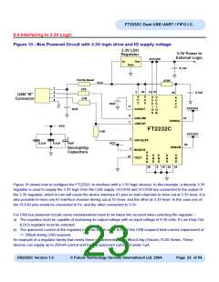
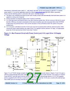
Figure 10 - Bus Powered Circuit with 3.3V logic drive and IO supply voltage
3.3V LDO
Regulator
VCC3V3
3.3V Power to
External Logic
In
Out
Gnd
0.1uF
Ferrite Bead
27R
470R
VCC
1
2
3
4
42
31
14
3
46
0.1uF
USB "B"
V
C
C
V
C
C
V
V
C
C
I
A
27R
Connector
C
C
I
V
C
C
33nF
6
VCC3V3
10nF
3v3OUT
O
A
O
B
8
7
USB DM
USB DP
10
SI/WUA
VCC
FT2232C
1.5K
VCC3V3
+
5
RSTOUT#
0.1uF
0.1uF
10uF
VCC
26
SI/WUB
Decoupling
Capacitors
4
RESET#
A
G
N
D
G
N
D
G
N
D
G
N
D
G
N
47
TEST
D
45
9
18 25 34
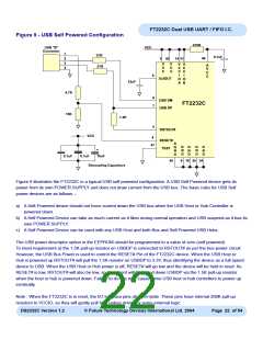
Figure 10 shows how to configure the FT2232C to interface with a 3.3V logic devices. In this example, a discrete 3.3V
regulator is used to supply the 3.3V logic from the USB supply. VCCIOA and VCCIOB are connected to the output of
the 3.3V regulator, which in turn will cause the device interface IO pins on both channels to drive out at 3.3V level. It is
also possible to have one IO interface channel driving out at 5V level, and the other at 3.3V level. In this case one of
the VCCIO pins would be connected to 5V, and the other connected to 3.3V.
For USB bus powered circuits some considerations have to be taken into account when selecting the regulator –
a) The regulator must be capable of sustaining its output voltage with an input voltage of 4.35 volts. A Low Drop Out
(LDO) regulator must be selected.
b) The quiescent current of the regulator must be low in order to meet the USB suspend total current requirement of
<= 500μA during USB suspend.
An example of a regulator family that meets these requirements is the MicroChip (Telcom) TC55 Series. These
devices can supply up to 250mA current and have a quiescent current of under 1μA.
DS2232C Version 1.2
© Future Technology Devices International Ltd. 2004
Page 23 of 54

 FTDI [ FUTURE TECHNOLOGY DEVICES INTERNATIONAL LTD. ]