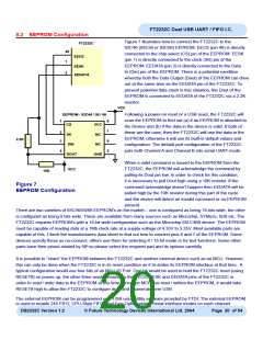
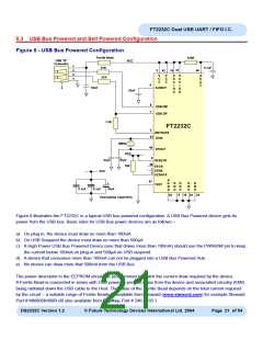
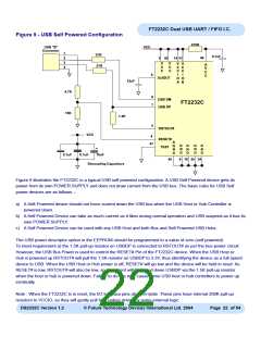
FT2232C Dual USB UART / FIFO I.C.
In some cases, where only a small amount of current is required (< 5mA) , it may be possible to use the in-built
regulator of the FT2232C to supply the 3.3V without any other components being required. In this case, connect
VCCIOA or VCCIOB to the 3V3OUT pin of the FT2232C.
Note : It should be emphasised that the 3.3V supply for VCCIO in a bus powered design with a 3.3V logic interface
should come from an LDO which is supplied by the USB bus, or from the 3V3OUT pin of the FT232BM, and not from
any other source. Please also note that if the SI/WU pins are not being used they should be pulled up to the same
supply as their respective VCCIO pin.
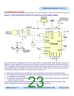
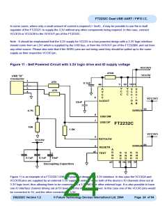
Figure 11 - Self Powered Circuit with 3.3V logic drive and IO supply voltage
VCC3V3
470R
VCC5V
USB "B"
Connector
1
27R
0.1uF
3
42 14 31
V
2
3
4
46
V
C
C
A
V
C
C
V
V
C
C
I
27R
C
C
C
I
C
6
VCC3V3
O
B
O
A
3v3OUT
33nF
10
SI/WUA
4.7K
8
7
USB DM
USB DP
FT2232C
10K
1.5K
VCC3V3
5
RSTOUT#
RESET#
VCC5V
26
SI/WUB
4
A
47
G
N
D
G
N
D
G
N
D
G
N
D
G
N
D
TEST
+
0.1uF
0.1uF
10uF
25 34
9 18
45
Decoupling Capacitors
Figure 11 is an example of a FT2232C USB self powered design with 3.3V interface. In this case the VCCIOA and
VCCIOB pins are supplied by an external 3.3V supply in order to make both of the device’s IO channels drive out at
3.3V logic level, thus allowing them to be connected to a 3.3V MCU or other external logic. It is also possible to have
one IO interface channel driving out at 5V level, and the other at 3.3V level. In this case one of the VCCIO pins would
be connected to 5V, and the other connected to 3.3V.
DS2232C Version 1.2
© Future Technology Devices International Ltd. 2004
Page 24 of 54

 FTDI [ FUTURE TECHNOLOGY DEVICES INTERNATIONAL LTD. ]