Ethernet: Three-Speed,10/100, MII Management
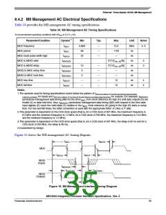
8.4.2 MII Management AC Electrical Specifications
Table 34 provides the MII management AC timing specifications.
Table 34. MII Management AC Timing Specifications
At recommended operating conditions with OVDD is 3.3 V 5%.
Parameter/Condition
MDC frequency
Symbol 1
Min
Typ
Max
Unit
Notes
fMDC
tMDC
0.893
96
—
—
—
10.4
MHz
ns
2, 4
MDC period
1120
MDC clock pulse width high
MDC to MDIO valid
MDC to MDIO delay
MDIO to MDC setup time
MDIO to MDC hold time
MDC rise time
tMDCH
32
—
ns
tMDKHDV
tMDKHDX
tMDDVKH
tMDDXKH
tMDCR
2*[1/(fccb_clk/8)]
ns
3
3
10
5
—
—
—
—
—
2*[1/(fccb_clk/8)]
ns
—
—
10
10
ns
0
ns
—
—
ns
4
4
MDC fall time
tMDHF
ns
Notes:
1.The symbols used for timing specifications herein follow the pattern of t(first two letters of functional block)(signal)(state)
(reference)(state) for inputs and t(first two letters of functional block)(reference)(state)(signal)(state) for outputs. For example, tMDKHDX
symbolizes management data timing (MD) for the time tMDC from clock reference (K) high (H) until data outputs (D) are
invalid (X) or data hold time. Also, tMDDVKH symbolizes management data timing (MD) with respect to the time data
input signals (D) reach the valid state (V) relative to the tMDC clock reference (K) going to the high (H) state or setup
time. For rise and fall times, the latter convention is used with the appropriate letter: R (rise) or F (fall).
2.This parameter is dependent on the CCB clock speed (that is, for a CCB clock of 267 MHz, the maximum frequency is
8.3 MHz and the minimum frequency is 1.2 MHz; for a CCB clock of 333 MHz, the maximum frequency is 10.4 MHz
and the minimum frequency is 1.5 MHz).
3.This parameter is dependent on the CCB clock speed (that is, for a CCB clock of 267 MHz, the delay is 60 ns and for a
CCB clock of 333 MHz, the delay is 48 ns).
4.Guaranteed by design.
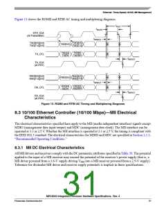
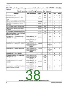
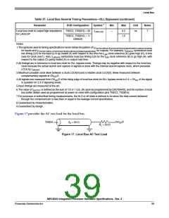
Figure 16 shows the MII management AC timing diagram.
tMDCR
tMDC
MDC
tMDCF
tMDCH
MDIO
(Input)
tMDDVKH
tMDKHDV
tMDDXKH
MDIO
(Output)
tMDKHDX
Figure 16. MII Management Interface Timing Diagram
MPC8540 Integrated Processor Hardware Specifications, Rev. 4
Freescale Semiconductor
35

 FREESCALE [ Freescale ]